Photovoltaics International Papers

Premium
Materials, Photovoltaics International Papers
With the transition of the cell structure from aluminium back-surface field (Al-BSF) to passivated emitter and rear cell (PERC), the efficiency of multicrystalline silicon solar cells becomes more and more sensitive to variations in electrical material quality. Moreover, the variety of multicrystalline materials has increased with the introduction of high-performance multicrystalline silicon. For these reasons, a reliable and verifiable assessment of the electrical material quality of multicrystalline wafers gains importance: to this end, a rating procedure based on photoluminescence imaging has been developed.
Premium
Fab & Facilities, Photovoltaics International Papers
With global business an increasing reality for PV, the role of logistics is transforming from service provider to true partner. This article makes the case for integrated partnership to move plant, products and business in the right direction.
Premium
Fab & Facilities, Photovoltaics International Papers
This report focuses on expansion announcements in the third quarter of 2015, which was expected to be the low point in new capacity expansion announcements. Momentum seen during the first half of the year, however, carried through, and so a full nine-month analysis is also provided, to further characterize developments in 2015.
Premium
Market Watch, Photovoltaics International Papers
The global PV capacity reached 177GW at the end of 2014, and by 2020 the PV Market Alliance forecasts that 630GW of PV could be installed. The entire value chain of the PV industry needs accurate data and a clear vision of how markets could develop in the future in order to avoid repeating past mistakes, and especially the damaging price war that led to a dramatic industry consolidation. The question of PV market evolution will be acute in 2015 and 2017, which will represent the next two important milestones for PV development: for the first time in years, the PV industry could approach its production capacity limits.
Premium
Photovoltaics International Papers, PV Modules
Newly developed high UV light transmission ethylene vinyl acetate (EVA) has recently been extensively introduced for use in PV modules. It has been proved that this type of EVA can result in potential power gain because of the better blue light response of the solar cell, which in turn can further reduce the cost per watt of the PV module. However, if only high UV transmission EVA is used as an encapsulant, too much UV light irradiates the backsheet, which can cause the backsheet to yellow. In order to improve the reliability and durability of the modules, SUNTECH, as a module manufacturer, therefore uses combined EVA, i.e. high UV transmission EVA as the front encapsulant and conventional UV cut-off EVA as the rear encapsulant, to protect the UV-sensitive backsheet. This paper presents the results of an investigation of the reliability and durability of high UV transmission EVA in PV modules, through an enhanced UV test which exceeds IEC standards.
Premium
Photovoltaics International Papers, PV Modules
One of the main concerns of module manufacturers is the power loss that takes place when the solar cells are incorporated in PV modules. This power loss, known as cell-to-module (CTM) loss, results from the influence of many factors which occur during module production. Some of these factors lead to a gain in power at the end of the process; on the other hand, some are responsible for a loss of power and offset the positive effects of other ones, resulting in a net power loss. In this paper the CTM losses will be addressed from an industrial point of view and for standard crystalline PV modules. The focus will first be on some of the most frequent issues detected in production lines and their influence on module power loss. More extensive research is then carried out to arrive at an explanation of their origin. This paper describes some of the mentioned factors along with the different ways of detecting them.
Premium
Photovoltaics International Papers, Thin Film
Of the various copper indium gallium diselenide (CIGS)-formation processes, a so-called ‘two-stage process’, consisting of sputtering and selenization, has been successfully applied in large-scale production thanks to its stable process scheme and high-fidelity production equipment. A CIGS module with a power of 231W, corresponding to a total area-based efficiency of 16% for 902mm × 1,602mm, was demonstrated when this twostage process was employed in a pilot production line at Samsung (although all the technology concerning CIGS production has now been transferred to Wonik IPS, whose main business is to provide production equipment for the semiconductor and display industry). The high-power module suggests significant potential for CIGS modules to compete with multicrystalline Si modules in terms of both cost and performance. This paper addresses the important process technologies for achieving high efficiency on large-area substrates, and presents a cost analysis using the data obtained from the operation of the pilot production line. As a result of the synergistic effect of low material cost and high efficiency of the two-stage process, the CIGS manufacturing cost is expected to be reduced to US$0.34/W.
Premium
Photovoltaics International Papers, Thin Film
With the introduction of the alkali post-deposition treatment (PDT) for the absorber layer in Cu(In,Ga)Se2 (CIGS)-based solar cells, new efficiency records approaching 22% have become feasible. After gallium incorporation, sodium doping and the three-stage process, this is the next milestone on the CIGS roadmap. In this paper the current understanding of how PDT alters the CIGS surface and affects device parameters is illustrated. A comparative study of cell device parameters from ZSW and the evolution of efficiencies from other institutes and companies with and without PDT is presented.
Premium
Cell Processing, Photovoltaics International Papers
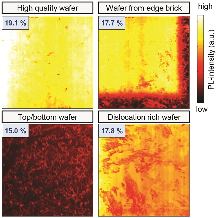
Interdigitated back contact (IBC) Si solar cells can be highly efficient: record efficiencies of up to 25.0%, measured over a cell area of 121cm2, have been demonstrated on IBC solar cells by SunPower. The high efficiencies achieved can be attributed to several advantages of cells of this type, including the absence of front metal grid shading and a reduced series resistance. Several metallization schemes have been reported for IBC cells, including screen-printing pastes, and physical vapour deposition (PVD) metal and Cu plating with a suitable barrier layer. In the IBC process development at imec, upscaling from small-area 2cm × 2cm cells to full-area 15.6cm × 15.6cm cells was carried out. In the first instance the 3μm-thick sputtered Al metallization scheme from the 2cm × 2cm cells was adopted. This resulted in cell efficiencies of up to 21.3%, limited by a fill factor (FF) of 77.4%. Besides the limited conductivity of this metallization, the sputtering of a thick Al layer is not straightforward from an industrial perspective; moreover, an Al cell metallization cannot be easily interconnected during module fabrication. A Cu-plating metallization for the large-area IBC cells was therefore investigated, and the scheme is described in detail in this paper. A suitable thin sputtered seed layer for the plating process was studied and developed; this layer serves as a barrier against Cu and has good contact properties to both n+ and p+ Si. The sputtering of the various materials could cause damage to the underlying passivation layer and to the Si at the cell level, leading to a lower open-circuit voltage (Voc) and pseudo fill factor (pFF). Reduction of this damage has made it possible to obtain IBC cells with efficiencies of up to 21.9%, measured over the full wafer area of 239cm2.
Premium
Cell Processing, Photovoltaics International Papers
Parallel dispensing technology as an alternative front-side metallization process for silicon solar cells offers the possibility of increasing cell conversion efficiency by 2% rel. by the use of commercial silver pastes designed for screen-printing technology. This efficiency gain is achieved through a significantly reduced finger width, and hence reduced shading losses, in combination with substantially improved finger homogeneities and high aspect ratios that guarantee sufficient grid conductivity at reduced paste lay-down. In this paper Fraunhofer ISE’s development of a parallel dispensing unit that is integrated into an industrial, inline-feasible platform made by ASYS is discussed. A possible industrial application of the dispensing technology is supported by latest results from pilot processing as well as by basic economic considerations

Subscribe to Newsletter

Upcoming Events

Solar Media Events
May 21, 2025
London, UK
Solar Media Events
June 17, 2025
Napa, USA
Solar Media Events
July 1, 2025
London, UK
Solar Media Events
July 1, 2025
London, UK
Solar Media Events
July 8, 2025
Asia