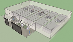
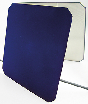
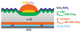
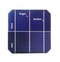
Photovoltaics International Papers

Premium
Photovoltaics International Papers, Thin Film
Most development work in the laboratory is dedicated to efficiency enhancements at the cell level; improvements in efficiency can lead to higher cost-competitiveness of PV. However, the cost of panel manufacturing is an important aspect as well. For CIGS panels the deposition of the active layer is an important part of the cost, and decreasing the layer thickness can reduce costs. Moreover, cost of ownership calculations can determine how much benefit can be expected from thinner absorber layers from a cost perspective; clearly, a thinner absorber will result in reduced absorption. To avoid losses, modelling can be used to predict the efficiency and viable light management strategies. Other efficiency-enhancing technology is related to the fact that most thin-film solar panels are monolithically interconnected. The area loss involved in this type of interconnection, and the trade-off between conductivity and transmittance of the front contact, impose limits on the maximum efficiency. The impact of improving both of these aspects is demonstrated in this paper. A viable way to improve the front contact is by supplementing the front contact with a metallic pattern. The benefit and the impact of different configurations and dimensions of the cell and metallic pattern are presented.
Premium
Cell Processing, Photovoltaics International Papers
This paper gives an overview of the application of silicon epitaxy as a doping technology in bulk crystalline silicon solar cells. The large degree of flexibility in designing a doped profile in one process step, and the elegant way of locally creating doped regions, or simply achieving single-side doping by selective epitaxy, are presented. Other advantages – such as the absence of subsequent steps to drive in the doped region, to activate the dopants and to heal any damage or remove glassy layers – position the technology as a strong alternative to classical diffusion. Silicon epitaxy is possible on the flat and textured surfaces of solar material, and is compatible with cleaning sequences suited to industrial implementation. The integration of epitaxial layers in solar cells is capable of providing not only high efficiencies but also simplifications of the cell fabrication process, and, therefore, reductions in the cell cost of ownership (CoO). The proof of concept at the cell level has been demonstrated by the integration of boron-doped epitaxial emitters in n-type IBC and PERT solar cells: 22.8% efficiency for IBC (4cm2) and 21.9% for PERT (238.9cm2) devices have been obtained.
Premium
Materials, Photovoltaics International Papers
Extended crystal defects, such as grain boundaries and dislocations, have long been considered the main factors limiting the performance of multicrystalline (mc-Si) silicon solar cells. However, because the detrimental effects of these crystal defects are reduced as a result of improvements in the solidification process as well as in the feedstock and crucible quality, the degradation caused by boron–oxygen complexes is expected to be of increasing importance. Light-induced degradation (LID) occurs in both p- and n-type crystalline silicon solar cells that contain both boron and oxygen. Because of the fundamental differences in the solidification processes, mc-Si silicon contains less oxygen than Czochralski silicon; nevertheless, the oxygen content in mc-Si silicon is still sufficient to cause degradation, although to a lesser extent than in the case of Czochralski silicon. Whereas B–O-related degradation of 0.5 to 1% abs. can be found in Czochralski cells, the degradation in conventional mc-Si cells is limited to around 0.1 to 0.2% abs.
Premium
Photovoltaics International Papers, PV Modules
In the last few years PV technology has seen continuous improvements, with significant enhancements at the cell and module levels. In addition to the requirement of high efficiency, the long-term reliability of PV modules leads to proposals for innovative module concepts and designs. Meyer Burger has developed a low-temperature wire-bonding technology, known as SmartWire Connection Technology (SWCT), with the aim of offering a cost-effective solution for high-efficiency solar cells while minimizing cell-to-module losses. The introduction of this interconnection design immediately brings new challenges, especially in the selection of an appropriate encapsulant, which must ensure a good processability as well as the required long-term module reliability. The compatibility of the most cost-effective types of encapsulant currently available on the market was analysed in the study reported in this paper. Thermoplastic polyolefin encapsulants with water absorption less than 0.1% and no (or few) cross-linking additives have proved to be the best option for long-lasting PV modules in a glass-glass (GG) configuration. The development of a laminator having a symmetrical structure (two heating plates without any vacuum membrane) has also opened the door to fast lamination processes with cycle times under eight minutes.
Premium
Photovoltaics International Papers, Thin Film
The current standards (IEC 61646 and IEC 61730-2, and IEC 62804 draft for c-Si only) are clearly insufficient to guarantee satisfactory long-term stability and energy yield for thin-film modules, given that reports from the field, as well as from laboratory test results (beyond IEC testing), in some cases show significant degradation of IEC-certified modules. Accordingly, thin-film modules can also exhibit degradation effects, such as TCO corrosion and power degradation, because of potential-induced degradation (PID). This paper presents the results obtained for thin-film modules subjected to bias and damp-heat (BDH) conditions in both indoor and outdoor tests. In order to assess module lifetimes for different thin-film technologies with respect to PID, indoor- and outdoor-determined leakage currents are compared and analysed, taking into account weather data and results from accelerated ageing tests. Finally, on the basis of simulations and investigations for different installation locations, module lifetimes are estimated and discussed.
Premium
Market Watch, Photovoltaics International Papers
Sophia, a four-year European Commission-funded project to promote coordination across the EU's PV research community came to an end in January. With 20 partners drawn from industry and academia, the project appears to have fulfilled its aims of fostering greater collaboration. But with Europe's PV manufacturing industry facing a dire predicament in the face of competition from Asia, is it too little, too late?
Premium
Materials, Photovoltaics International Papers
A shift from free-abrasive/steel wire sawing to fixed-abrasive diamond wire sawing is expected to take place in the PV cell manufacturing industry, with 2018 being the anticipated pivotal point for market dominance. This shift is due to several key advantages of diamond wire sawing, such as higher throughput, less wire per wafer, no slurry and the possibility of kerf recycling. However, in order for diamond wire sawing to realize its promise as the next-generation workhorse for the slicing of silicon PV wafers, inherent fundamental challenges must be properly identified and successfully addressed by the PV industry. As a first step to increasing the current collective understanding of the critical needs/challenges of diamond wire sawing, the c-Si programme of the U.S. PVMC held a workshop on July 8th, 2014 in San Francisco, California. One of the key products of this workshop was an extensive list of short- and long-term challenges. This article expands on some of the most important challenges identified at the workshop through the collective discussions and dialogue among a variety of PV industry experts and stakeholders.
Premium
Fab & Facilities, Photovoltaics International Papers
The manufacturers of silicon wafer solar cells are constantly looking into cost-effective ways to increase the efficiency of their solar cells. Most of these enhancements result from incremental improvements and can be achieved by optimizing existing processes. However, it is widely recognized that in order to further improve the silicon wafer solar cell efficiency, new solar cell architectures are required. This will in turn require new manufacturing processes, which will typically involve new production equipment and consumables. New consumables can play an important role in the applicability or success of a new process step; in this paper a specific focus will be on the precursors used for the deposition of surface passivation films, such as silicon nitride and aluminium oxide.
Premium
Fab & Facilities, Photovoltaics International Papers
In edition 26 of Photovoltaics International the rebirth of PV manufacturing capacity expansions in 2014 was analysed; this covered announcements on a global basis from a wide range of companies and included thin film and dedicated solar cell and module assembly lines, as well as integrated cell and module assembly lines. Because of the current level of capacity expansion announcements, a roughly quarterly analysis of such plans will be undertaken during 2015.
Premium
Cell Processing, Photovoltaics International Papers
Ion implantation offers significant process simplification potential for the fabrication of back-junction back-contact (BJBC) solar cells. First, the number of high-temperature steps can be reduced to one when applying a co-annealing process which includes an in situ growth of a silicon oxide passivation layer. Second, the implanted regions can be patterned in situ by utilizing shadow masks. ISFH's results from evaluating both aspects are reported in this paper. With fully ion-implanted, co-annealed and laser-structured small- area cells, efficiencies of up to 23.41% (20mm x 20mm designated area) have now been achieved. It is shown that the excellent recombination behaviour of 156mm x 156mm BJBC cells patterned in situ implies a potential for realizing efficiencies greater than 23%; however, back-end issues have so far limited the efficiency to 22.1% (full-area measurement). Ion implantation can also be utilized for the doping of BJBC cells with carrier-selective junctions based on polycrystalline silicon. The current status of ISFH's work in this direction is presented.

Subscribe to Newsletter

Upcoming Events

Media Partners, Solar Media Events
September 2, 2025
Mexico City, Mexico
Solar Media Events
September 16, 2025
Athens, Greece
Solar Media Events
September 22, 2025
Bilbao, Spain
Solar Media Events
September 30, 2025
Seattle, USA
Solar Media Events
October 1, 2025
London, UK