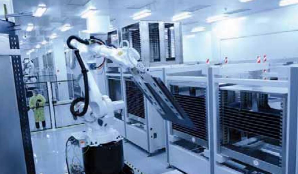
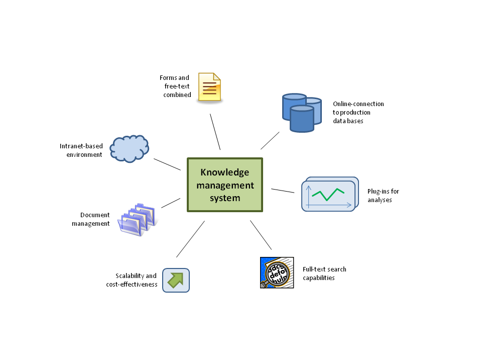
Supporting a smooth application of new wafer materials and handling equipment into photovoltaic mass production requires extensive testing of new wafers and equipments under a range of potential operating conditions. The management of such experiments, both in laboratory and production environments, demands the integration and management of a multitude of differing information. This includes static data-like equipment, specifications and experiment settings, online machine data regarding process signal and events – but also unstructured human knowledge, which is available in manual and test reports. To efficiently deal with these kind of complex environments, knowledge management techniques have proven to be a promising approach in various industrial applications. This paper depicts, by means of a photovoltaic wafer-testing platform at Fraunhofer IPA, how the application of automation systems and knowledge management techniques leads to more effective experiment management. More precisely, the gathered knowledge from the wider range of information included in the analysis of experiments can be re-used during future experiments and the manual effort is significantly reduced.