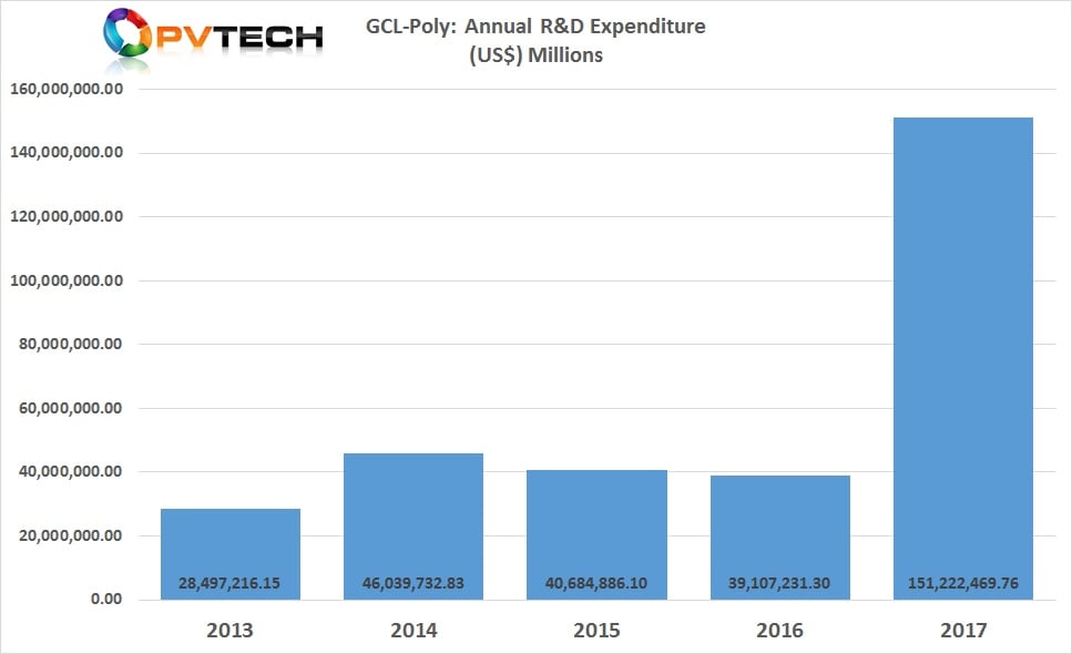
Leading polysilicon and solar wafer producer GCL-Poly Energy Holdings has reported a massive increase in R&D spending in 2017.
The company developed new mono-silicon crystal growth techniques and FBR (Fluidized Bed Reactor) technology as well as advances in diamond wire saw cutting and ‘Black Silicon’ wafer texturing for multicrystalline wafers.
Try Premium for just $1
- Full premium access for the first month at only $1
- Converts to an annual rate after 30 days unless cancelled
- Cancel anytime during the trial period
Premium Benefits
- Expert industry analysis and interviews
- Digital access to PV Tech Power journal
- Exclusive event discounts
Or get the full Premium subscription right away
Or continue reading this article for free
GCL-Poly’s R&D expenditure increased from RMB 247.29 million (US$39.1 million) in 2016 to RMB 956.13 million (US$151.22 million) in 2017, an increase of 288%.
The significant increase in R&D spending was principally cited by GCL-Poly in its 2017 annual report for impacting overall gross profit, which declined 45.5% to RMB 1,263.6 million US$199.7 million.
Monocrystalline R&D activities
GCL-Poly noted that after the acquisition the polysilicon material technologies from SunEdison including FBR and the constant Czochralski mono-silicon (CCZ) technologies, the company applied the technologies on custom made, lower cost domestic made equipment, which will be used at new high-volume facilities under construction in Xinjiang, China.
The CCZ technology and equipment are designed to meet demand and low-cost production for P-type monocrystalline and N-type monocrystalline wafers, while meeting semiconductor grade requirements of high-efficiency P-type mono PERC (Passivated Emitter Rear Cell) solar cells and IBC (interdigitated back contact) and heterojunction (HJ) solar cells requiring N-type mono wafers.
R&D activities included CCZ ‘heat shielding’ technology with low energy consumption as well as high speed ingot pulling and large feed capacity technology.
Multicrystalline R&D activities
As the largest multicrystalline ingot and wafer producer in the world, GCL-Poly highlighted that R&D and implementation activities in diamond wire saw cutting and ‘Black Silicon’ wafer texturing with the aim of completely migrating all production capacity to the two interrelated technologies had been the “biggest spotlights of GCL-Poly in 2017.”
GCL-Poly said that it had completed the upgrade of all wafer slicers to significantly reduce the wafer processing cost and that after the introduction of its first-generation ‘TS’ double-sided black silicon products it had launched the second-generation ‘TS+’ single-sided black silicon products. TS+ was said to have been developed to reduce “suede-surface” on the wafers, reducing texturing costs and facilitated widespread adoption of PERC cell technology on multicrystalline wafers.
Polysilicon R&D activities
R&D activities also focused on automation and ‘informatization’ of production processes, including intelligent manufacturing techniques and procedures to boost production efficiencies.
The company was able to increase polysilicon output by around 7.9% due to these measures, which resulted in approximately 74,818MT of polysilicon production in 2017, while nameplate remained at 70,000MT.
Backing-up its increase in R&D spending, GCL-Poly highlighted that it had applied for a total of 133 patents in 2017, which included 49 ‘invention patents’, and obtained 120 patent licenses.
Cumulative patent applications stood as 1,054 with 637 patents granted of which 289 were said to be invention patents.


