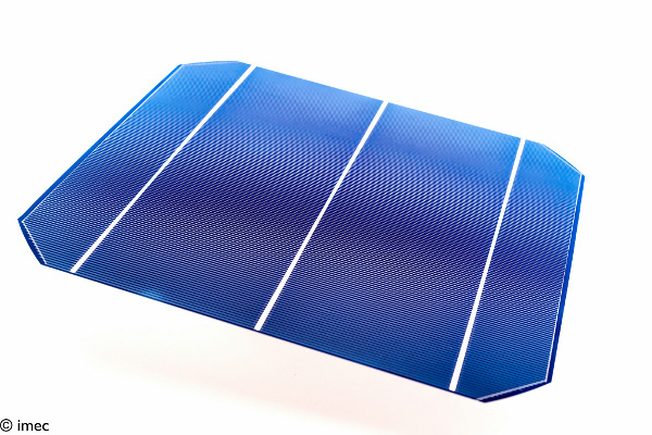
Nanoelectronics research center imec and kerfless epitaxial wafer start-up, Crystal Solar have demonstrated a homojunction solar cell with a record 22.5% conversion efficiency said to pave the way to low-cost solar wafer commercialisation.
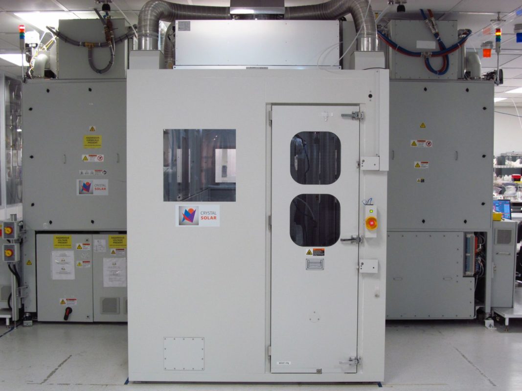
The potentially disruptive wafer technology was used to fabricate a standard monocrystalline156x156mm2 cell on 160um to 180um thick grown n-type wafer with built-in rear p+ emitter.
Try Premium for just $1
- Full premium access for the first month at only $1
- Converts to an annual rate after 30 days unless cancelled
- Cancel anytime during the trial period
Premium Benefits
- Expert industry analysis and interviews
- Digital access to PV Tech Power journal
- Exclusive event discounts
Or get the full Premium subscription right away
Or continue reading this article for free
Imec’s n-PERT process included a selective front surface field realized by laser doping, advanced emitter surface passivation by Al2O3 and Ni/Cu plated contacts, generating a record high Voc of 700mV, demonstrating the high quality of the ‘Direct Gas to Wafer’ technology and built-in junction. The cell efficiency was said to have been certified by FhG ISE CalLab.
Jozef Szlufcik, PV Department Director at imec said, “The combination of our advanced cell process and the innovative wafer manufacturing technique of Crystal Solar, is paving the way to the manufacturing of highly efficient solar cells at lower cost than currently possible. Using these kerfless wafers will be disruptive for the complete solar cell manufacturing value chain.”
T.S. Ravi, CEO of Crystal Solar added, “The epitaxial direct wafer growth with built in junctions approach represents a new paradigm in cell manufacturing with its unique ability to bypass significant steps in both wafer and cell manufacturing thereby dramatically reducing the capex and the overall cost per watt. We expect to achieve >23% efficiencies with IMEC’s PERT technology in the very near future.”
Although cell efficiency figures are important to demonstrate the technology also has to be low-cost, high-volume with high repeatability for industrial-scale production. The ‘Direct Gas to Wafer’ enables direct conversion of feedstock gas to monocrystalline silicon wafers by an epitaxial growth process, eliminating the need for crystal pulling ingots and the wire-sawing steps.