A research consortium has devised a proof of concept for a production line with a throughput of 15,000 to 20,000 wafers per hour, which is double the usual amount.
The group of plant manufacturers, metrology companies and research institutions is being led by the Fraunhofer Institute for Solar Energy Systems ISE and was established to reduce production costs and alleviate supply bottlenecks as a means to deploy increasing amount of solar.
Try Premium for just $1
- Full premium access for the first month at only $1
- Converts to an annual rate after 30 days unless cancelled
- Cancel anytime during the trial period
Premium Benefits
- Expert industry analysis and interviews
- Digital access to PV Tech Power journal
- Exclusive event discounts
Or get the full Premium subscription right away
Or continue reading this article for free
This would not only improve efficiencies and costs, the researchers said, but also render European manufacturing more competitive with China as the region looks to establish its own PV production infrastructure.
The doubling of throughput was down to “improvements to several individual process steps”, said the researchers, who will be presenting details of their results at this week’s eighth World Conference on Photovoltaic Energy Conversion in Milan, Italy.
New methods saw researchers enact an ‘on-the-fly laser equipment’, which allows high speed processing of large wafers as they move at speed under the laser scanner, as well as rotary screen printing instead of the current standard process of flatbed screening for the metallisation of solar cells.
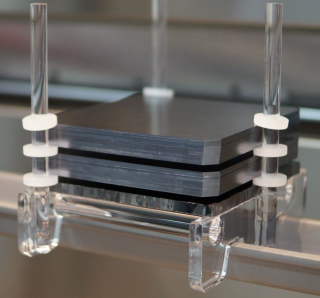
The researchers also sought to improve stack diffusion and oxidisation. Solar cells require differently doped sections and the researchers combined the diffusion process and the thermal oxidisation of the wafers into one step, meaning wafers are no longer placed individually but stacked on top of each other to be processed in the furnace. This resulted in throughput increasing by a factor of 2.4.
Next, they looked to establish faster inline furnace processes. Standard furnace processes in which the silicon solar cell is formed on both sides in inline furnaces require a substantial heating chamber to increase throughput. Instead, the consortium employed a belt speed that was three times faster and resulted in a significant ramp up in throughput without compromising the efficiency of the solar cell.
Finally, for the characterisation of the complete solar cells, the consortium devised two concepts: a contactless method and a method using sliding contacts. “This makes it possible to keep up a continuous speed of 1.9 meters per second while measuring the cells, with the team demonstrating great measurement accuracy for both concepts,” the consortium said, adding that a patent had been filed for the contactless method.
“In 2021, 78% of all silicon solar cells were produced in China,” explained Ralf Preu, division director of PV Production Technology at Fraunhofer ISE. “In order to deploy more solar installations as quickly as possible and to make our supply chains more robust, Europe should re-establish its own production centres for high-efficiency solar cells. “
“By boosting throughput and making production technology more resource-efficient, we can cut costs considerably and unlock sustainability potential that we will be able to leverage thanks to process knowledge and engineering excellence.”
“For some processes, established production workflows needed to be accelerated, other processes needed to be reinvented from scratch,” said Florian Clement, project manager at Fraunhofer ISE, which recently laid claim to a new solar cell efficiency record of 47.6%. “Compared to the numbers we currently see, the production systems developed within the scope of the project achieve at least double the throughput.”
The wafer format used in the experiment was not disclosed by Fraunhofer ISE but PV Tech understands that it was based on n-type technology.


")
