
As part of PV-Tech’s focus to understand the status of heterojunction (HJT) solar cell production, investments and field performance, PV Tech recently caught up with the CEO of Hevel Solar, Igor Shakhray.
Spread across two articles on PV-Tech, this is the first part, looking specifically at what has got Hevel to its position today as one of the leading HJT cell producers globally by volume. Many of the topics are also likely to feature at PV-Tech’s forthcoming PV HeterojunctionTech event in St. Petersburg on 18-19 November 2020.
Try Premium for just $1
- Full premium access for the first month at only $1
- Converts to an annual rate after 30 days unless cancelled
- Cancel anytime during the trial period
Premium Benefits
- Expert industry analysis and interviews
- Digital access to PV Tech Power journal
- Exclusive event discounts
Or get the full Premium subscription right away
Or continue reading this article for free
Thanks Igor for taking the time to catch up with PV-Tech. Can we start by going back to Hevel’s entry into the solar industry about 10 years ago? At this point, the entry strategy was similar to many new entrants at this time – thin-film. Why did the company invest initially in thin-film technology?
Igor Shakhray: “In the early 2010s major solar module manufacturers were driven by intention to avoid dependence on very high silicon prices at that moment.”
It took a few years before the thin-film panels were produced in any volumes. Was there still R&D to be done with the equipment delivered, or was this a sign that the thin-film efficiencies were too low to be competitive?
“As it was the first full-cycle solar module facility in Russia we faced some challenges from construction of manufacturing facility to its ramp-up. In parallel, we were running several R&D programs aimed at increasing efficiency and reducing the cost by the end of the ramp-up phase. We have learned much from that period, built up a professional team and acquired skills that are still valuable for the current and future R&D programs.”
The first time I came across Hevel’s move from thin-film to heterojunction silicon based activities was back in 2016, when European equipment suppliers announced sales deals for tools to Hevel. This would be a good time to understand first why Hevel decided to stay in the solar manufacturing sector, and why it was decided to set up heterojunction lines?
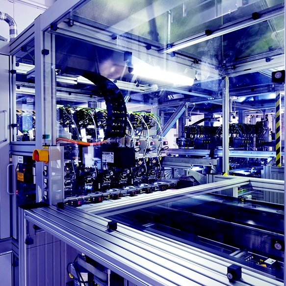
“By the time when thin-film technology started to decline worldwide due the dramatic fall of polysilicon prices we had already undertaken commitments to construct hundreds of megawatts of solar farms, we hired and trained personnel for all our business units – factory, R&D centre and engineering and construction . We were also encouraged by the results of R&D that confirmed that the most expensive part of the production lines, namely PECVD systems, could be applied in Si HJ technology, and they really proved record cell efficiency among Si based PV technologies. Furthermore PECVD is a low-temperature process. The simple structure of HJ solar cells, in combination with their high efficiency and low-temperature processing, makes them very attractive to the PV industry. This is the reason why we decided to transform existing micromorph module production line into a new HJT line.”
In terms of ramping up the first heterojunction lines, can you talk about the challenges? And what did you learn from setting up the a-Si thin-film activity before?
“PECVD process is the main one in a transformation of TF solar cell technology to heterojunction technology. The knowledge we gained by launching our thin-film line enabled us to make a swift transition to the heterojunction cell production. Nanometer-scale thicknesses of the PECVD films in HJT structures are really a challenge in terms of tuning of material properties of such films.
We also had to adapt the facilities that were initially built for the thin-film line. We partially maintained the existing process equipment, and the strong expertise of our team helped to integrate it into new processes and equipment.
One of the biggest challenges was to provide stable cell efficiency. We had been able to reach target in 3 months. Since then the cell efficiency has constantly been rising.”
When were heterojunction cell lines ramped up? What were the first challenges encountered in production?
“In April 2017 the ramp-up phase started with support of the in-house heterojunction solar cell technology developed by our own R&D centre and it took about three months to reach the target capacity. After reaching all the performance criteria and matching the process parameters at all process steps, we had to adjust the design of our solar power parks to the rapid growth of the cell efficiency and module power. The annual production capacity was increased from initial 97 MWp to 160 MWp during the first phase of the project. During the second phase of the project (June 2017 – May 2019), the production capacity was increased to 260 MWp and by March we completed the third phase, extending production capacity to 340 MWp.”
The utilization rates of the heterojunction lines have been impressive during the past couple of years. Are the lines today fully optimized in terms of throughput, or is there still scope to debottleneck and optimize further?
“In general, for HJT process still the PECVD process is the bottle-neck of the process, both in terms of CAPEX and production capacity, with typical production throughputs of 2400-3600 w/hour; meanwhile the industry standard for the tools shifts towards 6000 – 8000 w/hour. From the very beginning we have realized the critical step in the process and later we have successfully managed it through the two stages of expansion of the production capacity. Another challenge is cell thickness. Although its further reductions are also possible without significant losses in efficiency, the implementation of thinner wafers in mass production is currently limited by handling issues, resulting in excessive wafer breakage rates.”
Looking now at efficiencies, I assume this has been an area of constant improvement since the lines were first ramped up. Can you talk about production cell efficiencies over the past few years, leading up to typical averages today? What have been the key areas that have been improved on, to get to these efficiency levels?
“Having started the production at the level of about 21%, today we have average 23,4% in mass production. Most important areas we have focused on were the passivation quality and the interfaces between layers. However, this result could only be reached by elaborating every process and pushing every material characteristics to its best. And of course, it is very important to accurately tune the processes to stabilize cell characteristics along all production chain.”
Also on the cell side, of course the big issue in solar is cost. Perhaps this is a good time to move to module powers, as this is probably where gross margins are more relevant. Driving down module costs is key for all technologies in the solar industry. How has Hevel addressed cost-reduction, other than benefiting from lower costs buying in wafers?
“Actually there are several targets here. First is to constantly increase the module power which is directly related to cell efficiency. Second is of course to reduce the production losses and inefficient material usage, constantly optimize the bill of materials and avoid extra costs.”
Heterojunction is known to be a technology that lends itself very well to bifaciality. How has Hevel implemented bifacial capability in its cell and module lines?
“Our cells are bifacial from the very beginning of our production. This gives advantage in any module design – both glass-glass and glass-backsheet as well. We have implemented both glass-glass bifacial and glass-backsheet monofacial module designs on our production.”


