Cell Processing

Premium
Cell Processing, Photovoltaics International Papers
Among all of the tests performed in the production chain of solar cells, each with the scope of production control and the aim of driving engineering improvements, the electrical final test is certainly the most important. The final test defines the gate to module manufacturing and has a direct impact on finances and customer satisfaction. The test procedure itself is well known and continues to undergo constant further development, but that shall not be the scope of this article. This paper will elucidate on the issues faced by bringing these tests into high volume production, highlighting some issues on measurement accuracy and degradation of the internal calibration standards. In addition to pure electrical testing, the paper will discuss the Q-Cells approach to identifying hot spots and subsequent binning of the affected cells without adding process time to the test procedure, and will show their straightforward correlation to heat generation of these hot spots in real-life condition-encapsulated module tests.
Premium
Cell Processing, Photovoltaics International Papers
The PV industry is expected to eventually reduce its manufacturing costs well below €1/Wp. Major technological changes lie ahead of us for manufacturing wafers, solar cells and modules if this cost target is to be met. In order to focus R&D efforts amongst the myriad options, and to speed up the learning curve, the PV industry (equipment vendors, material suppliers and PV manufacturers) may benefit from collaborative efforts guided by an ITRS-like roadmap. In this paper we present the IMEC roadmap, the target of which is to reduce drastically the amount of pure Si needed per Wp by combining efficiencies beyond 20% with aggressive reductions in wafer thicknesses.
Premium
Cell Processing, Photovoltaics International Papers
In today’s market, crystalline silicon wafer technology dominates industrial solar cell production. Common devices feature opposing electrodes that are situated at the front and rear surface of the wafer and subsequent front-to-rear interconnection is used for module assembly. This paper reflects the functions which have to be fulfilled for the back-side contact of the solar cell as well as challenges and advances for the two basic classes: full-area and local rear contact formation. While full-area contacting has proven to be a reliable technology for industrial production, local contacting through dielectric layers has yet to be put through its paces in industrial implementation.
Premium
Cell Processing, Photovoltaics International Papers
This paper, the second in a series covering cost of ownership studies for photovoltaics [1], examines the need for saw damage removal and the follow-on processes of precleaning, texturization, and cleaning. The process considerations for wet and plasma approaches are further discussed before taking a detailed look at texturization using random pyramid formation. The paper will conclude with a view of current and future wet process techniques and a cost of ownership case study using Akrion Systems’ GAMA-Solar as an example.
Premium
Cell Processing, Photovoltaics International Papers
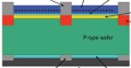
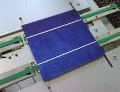
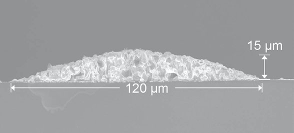
One-step screen-printing processes are still the most widely-used technique for the front-side metallization of crystalline silicon solar cells in the PV industry. This is because of the knowledge, stability and speed of the process, and despite some big disadvantages exhibited by the resulting contacts. Therefore, the metal contacts of high-efficiency laboratory cells are usually produced via advanced two-step metallization processes, which allow the application of optimized contact structures. In a first step, a narrow metal layer is applied to form the contact to the silicon wafer. Several different techniques have been developed for this first stage. In the second step, the seed layer is reinforced electrochemically with a dense layer of a metal of high conductivity, usually by light-induced plating. The transfer of such techniques into industrial scale has been pursued intensively, and may enter solar cell production lines in the near future. However, the process can still be improved based on a better process understanding, in order to benefit from the full potential of the technology.
Premium
Cell Processing, Photovoltaics International Papers
Standard solar cell technology nowadays offers a variety of measures - some linked, some not - to continuously improve conversion efficiency. The starting point for considering the different improvement steps is a kind of standard cell as produced on most current production lines. The main elements of this cell are diffused junction, aluminium back-surface field and screen-print metallization. This type of cell suffers losses from different sources like optics, recombination and resistance that can be considerably lowered to obtain higher cell efficiency. This paper will describe improvement steps on the standard type of multi-crystalline cell before addressing cell concepts that open further potential.
Premium
Cell Processing, Photovoltaics International Papers
Photovoltaic modules are designed to meet the reliability and safety requirements of national and international test standards. Qualification testing is a short-duration (typically, 60-90 days) accelerated testing protocol, and it may be considered as a minimum requirement to undertake reliability testing. The goal of qualification testing is to identify the initial short-term reliability issues in the field, while the qualification testing/certification is primarily driven by marketplace requirements. Safety testing, however, is a regulatory requirement where the modules are assessed for the prevention of electrical shock, fire hazards, and personal injury due to electrical, mechanical, and environmental stresses in the field. This paper examines recent reliability and safety studies conducted at TÜV Rheinland PTL’s solar module testing facility in Arizona.
Premium
Cell Processing, Photovoltaics International Papers
The key to delivering highly efficient solar cells is to absorb as much light as possible from the solar spectrum and convert it effectively into electrical energy. Anti-reflective coatings have served as agents for reducing reflective losses and improving bulk and surface passivation thus enhancing both of the parameters – short circuit current and open circuit voltage of a solar cell. Simulation studies show that an SiN/MgF dual-layer anti-reflective coating is best for a bare cell. This paper takes a closer look at how this coating can reduce the reflectance for a broad range of wavelengths and thus enhance the quantum efficiency of the cell in the blue and red region of the solar spectrum.
Premium
Cell Processing, Photovoltaics International Papers
Despite the fall in silicon prices, wafer thickness continues to be reduced. The handling of thin wafers between 120 and 160µm is under research at the Fraunhofer IPA, where gripper-dependent and independent variables were determined as parameters for the handling process. Diverse grippers are tested on an automated test platform. Among these are grippers that are specifically designed for wafer handling, as well as others that are not but are used for wafer manipulation. The test platform includes several different test and handling equipments and utilizes critical parameters that might be required for achieving a high production rate via shortest cycle times to investigate the impact on thin wafers. The first results of the position accuracy measurement in relation to the physical movement parameters and other industrial key figures in ongoing handling research are presented within this paper.
Premium
Cell Processing, Photovoltaics International Papers
Lowering the cost of production of solar cells requires higher throughputs and higher production yields for thinner and more fragile silicon wafers, and inline processing could hold the key. However, current processes used in production do not enable full inline processing and often require a substantial amount of handling between process stations as the throughputs per station and tray requirements differ greatly. It will take many years before a full inline process flow is available and if it comes, wafers will most likely be positioned on a single tray throughout all process stations. This paper will discuss the current processing methods for all individual process steps and will provide an outlook on inline processing in view of the three cost reduction strategies: thinner wafers, higher throughput, and higher efficiency cell designs.

Subscribe to Newsletter

Upcoming Events

Solar Media Events
April 10, 2024
Dallas, Texas USA
Solar Media Events
April 17, 2024
Lisbon, Portugal
Solar Media Events
May 1, 2024
Dallas, Texas
Solar Media Events
May 21, 2024
Napa, USA