One of the biggest trends in PV manufacturing today is the adoption of black silicon – a technology that has been talked about for years but has only recently started to be produced at scale. Some of the benefits like uniform black cells that absorb more light and produce more current are obvious – but other benefits in improving FF and Voc are more elusive as is reliably producing the right structures to enable the best possible cell efficiency. ASG’s team has been working on black silicon for over a decade and this article provides some insights into the technology gained from that experience.
In adopting black silicon, the industry had to overcome many challenges. One concern when this technology was first being explored, was that the nanotexture would not stay intact during the doping process. Since the nanotexture does survive the high temperature in the doping process, the nanotexture can be done before the diffusion step, which enables a shorter and higher throughput diffusion process. Many were also concerned that the small features of the nanotexture would increase the surface area and result in an unavoidably high surface recombination velocity. This also was overcome with a combination of device design and optimizing the geometry of the nanotexture.1,2 Other issues, such as screen printing to the nanotexture3 and using metal in such a way that it doesn’t degrade the cell performance were also solved.
Try Premium for just $1
- Full premium access for the first month at only $1
- Converts to an annual rate after 30 days unless cancelled
- Cancel anytime during the trial period
Premium Benefits
- Expert industry analysis and interviews
- Digital access to PV Tech Power journal
- Exclusive event discounts
Or get the full Premium subscription right away
Or continue reading this article for free
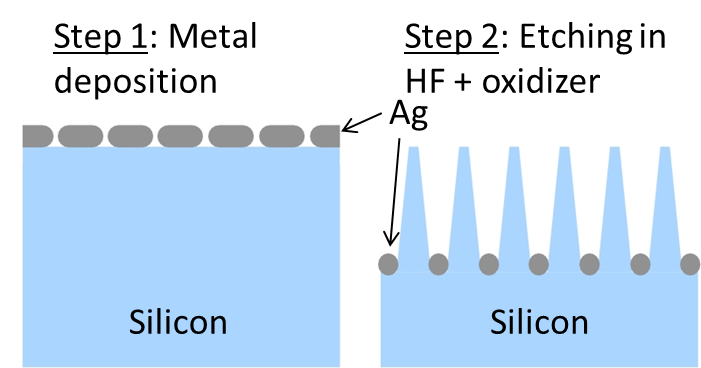
Now, the industry uses many different kinds of black silicon. Processes to nanotexture surfaces include variations of metal enhanced etching, RIE, and occasionally laser processing is used. Metal enhanced etching has the advantage that it can be high throughput. In addition, metal enhanced etching can be done in existing wet chemical process tools. Metal enhanced etching works by depositing a thin amount of metal onto a silicon wafer. The metal coated silicon is then exposed to a solution containing an oxidizer and hydrofluoric acid (HF). The silicon etches where the metal touches the silicon and does not etch it where the metal is blocked or not present from the silicon surface. See figure 1. While all metal enhanced etching has these steps in common, the details of the process change the results drastically. The processes vary on parameters such as the type of metal used, the way the metal is deposited onto the surface, the type of oxidizer used, the chemistry of the etch, and the processing conditions such as temperature and light exposure.4
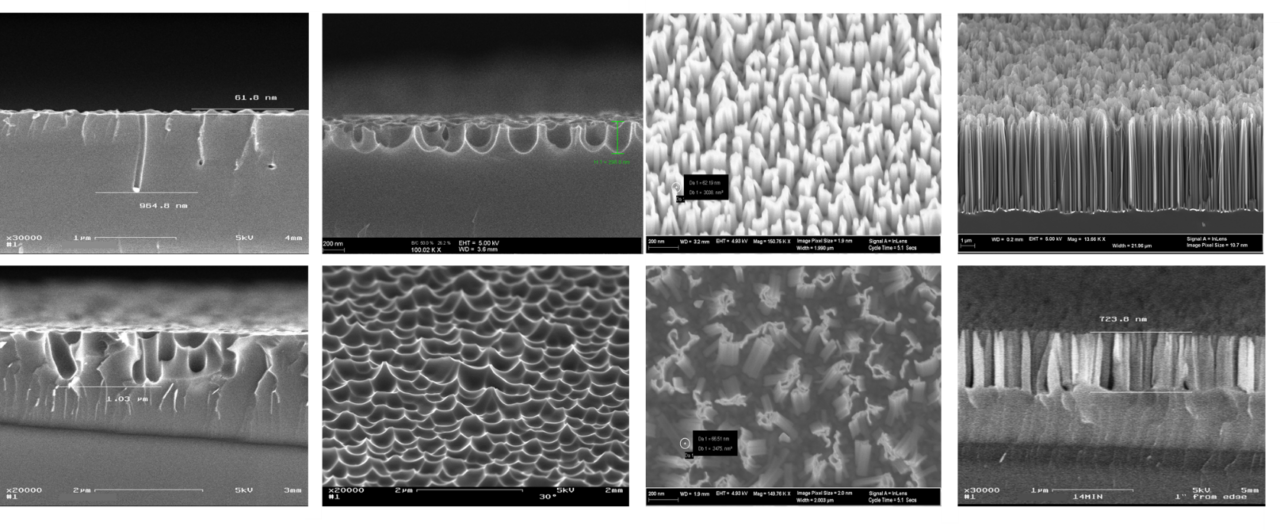
Black silicon refers to any nanotexture, but the geometry of the nanotexure can vary and small changes on the nanoscale have a large impact on the macroscale. For example, the density, taper, and the length of nanowires drastically alter the optical reflection and absorption of the module. Figure 2 shows some example of structures all made using metal enhanced etching.
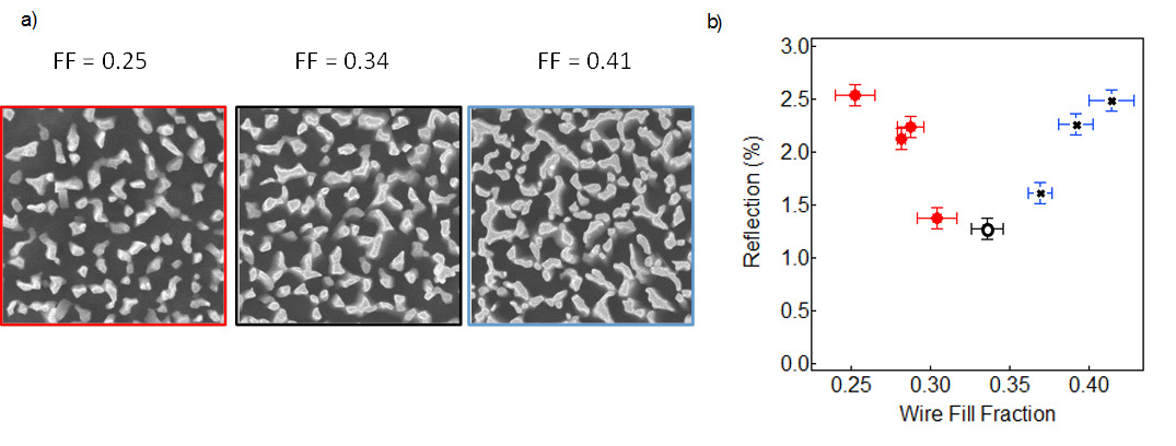
One of the key reasons for the increased in efficiency for black silicon solar cells is their lower reflection. So optimizing this low reflection is critical to realizing some of the benefits of black silicon solar cells. Since the structures are smaller than the wavelength of light, the light sees a combination of the silicon, passivation layer, and air as one material. For less dense nanostructures, as the light moves from the EVA to the tip of the nanostructures, the change is small and therefore the reflection is small. However, if the light is not completely scattered or absorbed by the time the light reaches the base of the nanowires, the transition to the underlaying bulk (non-nanostructured) silicon is abrupt and results in a large reflection from the base of the nanostructure. For densely packed nanotextures, the transition from the EVA to the top of the nanostructures will result in a reflection from the top surface. Figure 3 shows the reflection for nanowire arrays with the percentage of silicon (fill fraction) varying from 25% to 41%. The minimum reflection for this geometry of nanowires is 34% fill fraction while 41% is too large and 25% is too small. This is just one example of how sensitive optimization of the geometry of the nanotextured array is needed to achieve the optimal cell efficiency.
When designing the shape of the nanostructures much needs to be considered. Some considerations include:
- The tradeoff between deeper nanostructures (longer wires) and reflection. Getting a low reflection is trivial, but obtaining cells with low reflection and high efficiency, while possible, requires optimization.
- Avoiding porous silicon on top of the nanostructures. Certain metal enhanced etching processes form a porous silicon layer on top of the nanotexture. This porous silicon layer will lead to a dead region degrading the blue response and lowering efficiency.
- The nanostructure needs to be designed for optimal performance in the module/finished cell. This design is different than the structure that is optimized for a bare wafer. One example of this is that an oxide is formed during diffusion which changes the nanostructure. Also, depending on the type of SiN passivation, the optimal geometry of the nanotexture varies. In general, the optimized nanostructure process will depend on the details of the rest of the cell and possible module assembly processes.
- The nanostructure should be optimized for reliability and not just efficiency. For example, different nanostructures result in different adhesion of metal fingers and bus bars to the cell.
While many are using black silicon, the potential benefits far exceed what most are making use of. The benefits of black silicon go beyond enabling diamond wire sawn wafers. Efficiency boosts being reported are around 0.4%.5 While impressive for a new process at today’s cell efficiencies, it is likely further optimization could yield additional gains. A new material requires a new device design to make use of that material’s novel properties.6 Most cell manufactures have not yet optimized their cell process for nanotextured cells and thus are realizing only part of the benefits of these cells.
In addition to nanotextured traditional multi cells, black silicon could bring benefits to other cell structures as well. For mono crystalline cells, black silicon could enable cells designs without silicon nitride and with just using silicon dioxide or alumina to passivate the surface, since an anti-reflection layer is not required with black silicon. This cell design is especially relevant for higher efficiency designs that currently use both a passivating layer and an anti-reflection coating. In addition, metal enhanced etching can be a singled sided process leaving the backside smooth for high efficiency cell designs. Another advantage of black silicon, if properly designed, is the sharper features in some nanotextures can result in improved screen printing thus increasing fill factors and adhesion. Sharper features lead to better contacts.
Nanotextures can also be used in a low-cost process to remove passivation for metal contacts. By gently raking a metal comb over the surface of the nanowires, the tips of nanostructures can be cleaved off to expose the underlaying silicon. Metal contacts can then be deposited to this surface.7
We’ll likely see much wider adoption of black silicon in the coming years and more advanced concepts using this new material. ASG looks forward to helping the industry take full advantage of this potential.
References
1 Jura, M.P., et al. “Conventionally-processed silicon nanowire solar cells demonstrating efficiency improvement over standard cells,” Photovoltaic Specialist Conference (PVSC), 2014 IEEE 40th, 2014.
2 Modawar, F. et al., US 9099583: Nanowire device with alumina passivation layer and methods of making same USPTO, 2011, Advanced Silicon Group.
3 Jura, M., et al., US 20140332068: Screen printing electrical contacts to nanowire areas USPTO, 2012, Advanced Silicon Group.
4 Toor, Fatima, et al. “Nanostructured silicon via metal assisted catalyzed etch (MACE): chemistry fundamentals and pattern engineering,” Nanotechnology 27, 41, 2016, 412003.
5 Wang, X., et al. 19.31%-efficient multicrystalline silicon solar cells using MCCE black silicon technology, Photovoltaics International, 35, March 2017.
6 Toor, Fatima, et al. “Metal assisted catalyzed etched (MACE) black Si: optics and device physics,” Nanoscale, 8, 34, 2016, 15448-15466.
7 Black, M.R., et al., US 8852981: Electrical contacts to nanostructured areas, USPTO, 2011, Advanced Silicon Group.
Marcie R. Black, Co-Founder and CEO, Advanced Silicon Group
An expert on black silicon technology, having worked on nanostructured silicon for over 10 years and on nanostructured materials for 20 years, Dr. Black previously co-founded Bandgap Engineering, and worked at Los Alamos National Laboratory and Motorola. Marcie holds a Ph.D. from MIT in Electrical Engineering.
William B. Rever, III, Co-Founder and Chief Marketing and Sales Officer, Advanced Silicon Group
A 35 year veteran of the PV industry including roles at pioneer Solarex/BP Solar and as an independent consultant, Bill holds a B.A. in Physics from Johns Hopkins University, an MSE in Energy Engineering from the University of Pennsylvania, and an MBA from that University’s Wharton School of Business.


