
One of the key themes of PV CellTech 2017 is to understand exactly what is happening in n-type cell manufacturing today, and which companies are going to emerge as viable competition to SunPower, Panasonic and LG Electronics.
The past couple of years has seen a resurgence in n-type activity, and in the past few months also, a rather interesting turn of events that I will explain later in this blog.
Try Premium for just $1
- Full premium access for the first month at only $1
- Converts to an annual rate after 30 days unless cancelled
- Cancel anytime during the trial period
Premium Benefits
- Expert industry analysis and interviews
- Digital access to PV Tech Power journal
- Exclusive event discounts
Or get the full Premium subscription right away
Or continue reading this article for free
There are several n-type architectures that can be employed using n-type wafers, with interdigitated back-contact (IBC) and heterojunction (HJT) being the two cell types that move average cell efficiencies well into the >20% band.
Each has very well defined process stages, and until now, each of IBC and HJT has remained the exclusive domain of SunPower and Panasonic, respectively: but not through a lack of desire on other c-Si cell producers in wishing to produce premium efficiency.
In terms of the entrance barriers, it would seem that IBC cell technology is on a different level to HJT, and this likely explains why we have seen more announcements from new entrants into the HJT space recently. Only LG Electronics would appear to be positioning itself as being the ‘next’ viable IBC producer, but we are still at early stages of the company’s efforts to position itself here.
Rather, heterojunction lines are now the focus of many companies that are seeking to have a product offering that is beyond the reach of the very best PERC proponents in the industry. And interestingly, it is the equipment suppliers and research institutes that are the real drivers, not necessarily the cell producers.
The above narrative actually could have been written any time over the past 30 years of solar cell production. But today in 2017, we have a new dynamic underpinning heterojunction activity, and the basis for this is most unlikely.
Wind the clock back 10 years. The solar industry was very different, and many of the technology forecasts by industry analysts were founded on an inevitable shift to (then called Gen 2) thin-film technologies, and with a-Si based glass panels having significant market-share out to 2020.
The underlying premise of this was somewhat naïve of course, and if you looked behind the marketing rhetoric, you quickly realised that the case for a-Si panels was coming from PVD/PECVD tool suppliers from the displays industry that saw the solar industry as an attractive adjacent segment revenue stream.
However, during the uptick of turn-key a-Si lines, multi-GW of capacity was installed across a wide range of companies in Europe and Asia, with equipment suppliers Applied Materials, Oerlikon, ULVAC and Jusung flying high.
And then almost overnight, all the lines were deemed uncompetitive, with just getting to double-digit module efficiencies a challenge too hard for most.
But in the past couple of years, we have seen the PVD and PECVD tools being repurposed, as they are directly usable for heterojunction process steps, with the most recent being the third incarnation of STMicroelectronics original 300mm fab that was mothballed in 2009. The site was initially re-established by 3SUN (then the ‘3’ being Enel, Sharp and STMicroelectronics) as an a-Si PV fab, before Enel became the sole owner, initially feeding into part of Enel Green Power’s global EPC pipeline.
On 4 March 2017, Enel Green Power announced plans to convert the a-Si lines into bi-facial heterojunction lines.
The change from 300mm wafers to triple-junction a-Si PV production to c-Si bifacial heterojunction lines: this is something nobody could remotely have forecasted!
Could we be at the start of a major push to get more of the mothballed a-Si PVD/PECVD tooling brought back to life as c-Si heterojunction equipment? What a change that would make to solar cell manufacturing – multi GW of new n-type heterojunction capacity coming online with upgrade capex only?
Could this also be the catalyst that prompts (former AKT) Applied Materials business operations in Santa Clara to get back into solar, outside of the continued Baccini operations in Treviso? While this was potentially on the cards with the previous plans of the former Silevo operations in the US, a strong pull on its SunFab lines to be running as heterojunction lines could be an unexpected upside that was seen as highly unlikely a few years ago, and would play directly into the strengths of AMAT.
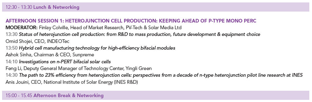
The afternoon of day-1 of PV CellTech in Penang on 14 March 2017 is therefore going to be fascinating with talks from Omid Shojei of INDEOtec, Ashkok Sinha of Sunpreme and Anis Jouini from the National Institute of Solar Energy (INES).
The talk from Anis Jouini is one that many of the attendees have expressed strong interest in, as providing key findings from more than 10 years of heterojunction pilot-line research.
Earlier this week, we caught up with Anis to hear about what he was intending for his talk at PV CellTech 2017.
What are you going to cover in the talk?
Anis Jouini: There will be mainly four parts in my talk: an overview about the PV industrial actors interested on heterojunction cell technology; the R&D progress at INES of heterojunction cell technology evolution since more than a decade; [the] main achievements on heterojunction cell pilot line taking into account the wafer type/effect and the module assembly technology (busbars and Smart Wire Technology); [the] compatibility of heterojunction cells with advanced technology (very thin wafers, flexible modules).
What challenges are you seeing with cell manufacturers today?
Moving to the premium class of cells with high efficiency 25% to 30% and more, and keeping/improving the productivity while using thin (and thinner) wafers. This means a few steps process which combines crystalline Si with other technologies.
What do you hope to learn from the PV CellTech event in Penang?
Strategic overview of the present and future market (of) PV cell technologies.
PV CellTech takes place on 14-15 March 2017 in Penang, Malaysia. To register to attend the event, please use this link.


