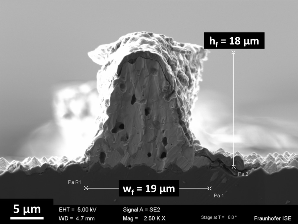
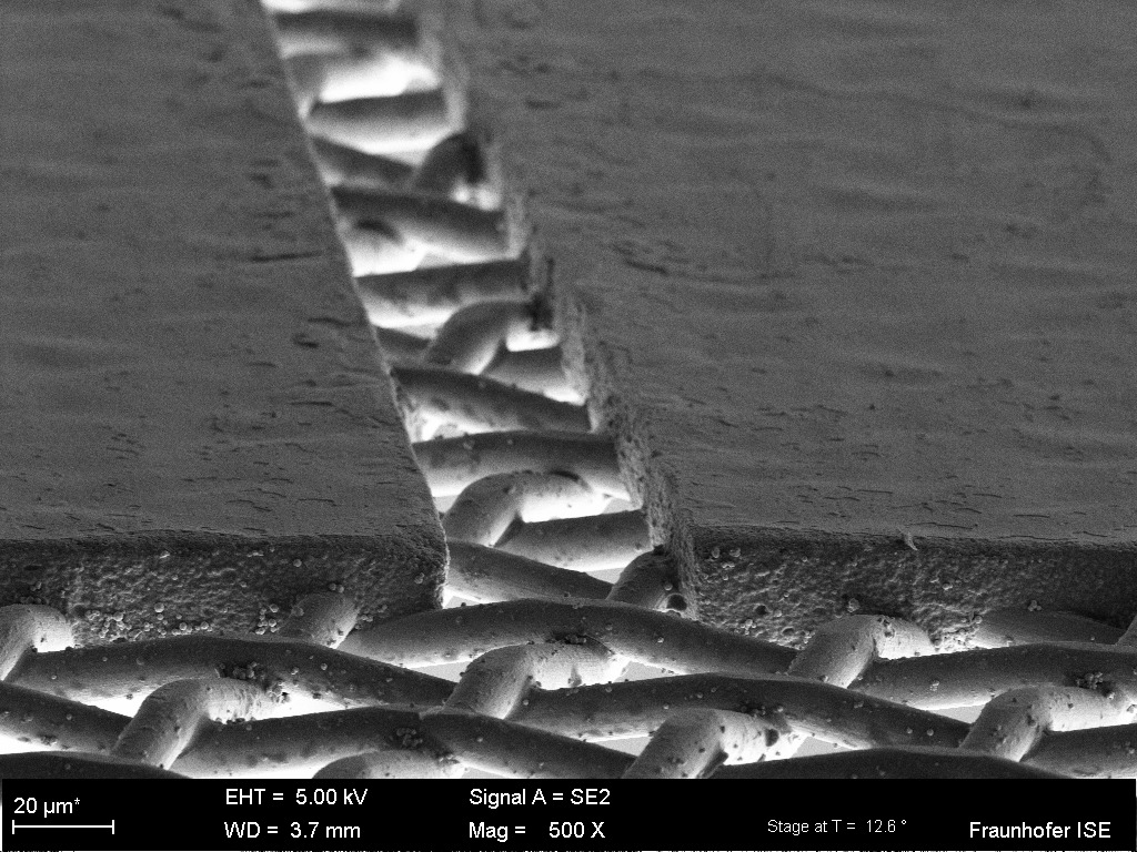
Fraunhofer ISE in collaboration with industrial partners have developed a fine-line metallisation process to create contact fingers with a width of 19µm and a height of 18µm in a single printing step that is almost invisible to the naked eye.
The collaborative project dubbed, ‘FINALE’ includes screen manufacturers Koenen and Murakami and screen chemical supplier, Kissel + Wolf. Optical inspection specialist, Wickon Hightech also participated in the project which was funded by funded by the German Federal Ministry for Economic Affairs and Energy BMWi.
Try Premium for just $1
- Full premium access for the first month at only $1
- Converts to an annual rate after 30 days unless cancelled
- Cancel anytime during the trial period
Premium Benefits
- Expert industry analysis and interviews
- Digital access to PV Tech Power journal
- Exclusive event discounts
Or get the full Premium subscription right away
Or continue reading this article for free
Dr.-Ing. Andreas Lorenz, project manager in the Printing Technology group at Fraunhofer ISE said, “Working together with industry partners in fine-line screen printing metallization, in particular with screen manufacturers Koenen GmbH and Murakami Co. Ltd. as well as screen chemical supplier Kissel + Wolf GmbH, we have managed to reduce the contact fingers’ width to less than 20 micrometers — a reduction of 30 to 40 percent compared with the current industry standard.”
Fraunhofer ISE said that innovative fine-mesh screens were used in the metallisation of passivated emitter and rear contact (PERC) solar cells in two independent test series that created contact fingers with a width of merely 19µm and a height of 18µm in a single printing step.
When integrated into modules that would be able to deploy multi-busbar interconnection with 8 to 15 busbars, higher electrical properties and lower power losses can be achieved, according to Fraunhofer ISE.
“Using highly engineered screen and paste systems for fine-line metallisation, it could be possible to start manufacturing solar cells with nearly invisible contact fingers on an industrial scale in the near future. This would represent a great advantage for applications in integrated photovoltaics, where aesthetic, homogeneous module surfaces are in demand,” added Dr. Florian Clement, Head of the Production Technology — Structuring and Metallisation Department at Fraunhofer ISE.
The results of these test series will be presented at two upcoming PV conferences — the 36th EU PVSEC in Marseille, France, and the 29th PVSEC in Xi’an, China.


