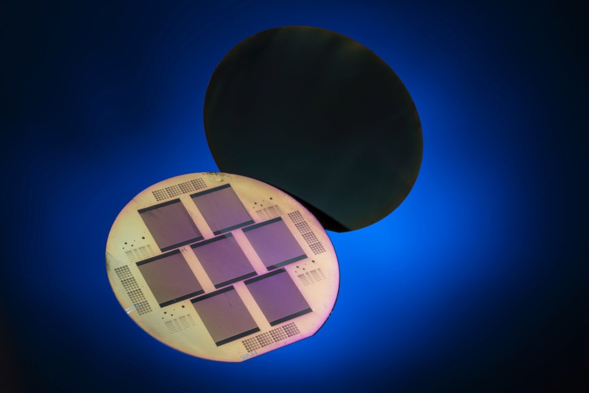
The Institute for Solar Energy Research Hamelin (ISFH) and the Leibniz Universität Hannover have produced lab cells using polysilicon on oxide – POLO – junctions, in an interdigitated pattern on the rear side and a specially treated p-type monocrystalline wafer to record a cell conversion efficiency of 26.1%.
Prof. Rolf Brendel, director of ISFH said, “Our result demonstrates that neither n-type silicon nor boron-diffusions, nor amorphous silicon are a must for ultra-high efficiencies. There are also other attractive pathways to highest efficiencies with silicon at potentially low cost!”
Try Premium for just $1
- Full premium access for the first month at only $1
- Converts to an annual rate after 30 days unless cancelled
- Cancel anytime during the trial period
Premium Benefits
- Expert industry analysis and interviews
- Digital access to PV Tech Power journal
- Exclusive event discounts
Or get the full Premium subscription right away
Or continue reading this article for free
The record cell was described as uses a passivating electron-selective n+-type polysilicon on oxide (POLO) junction at the minus contact of the cell and a hole-selective p+-type POLO junction at the plus contact.
The high selectivity of POLO junctions are a key factor in generating the high efficiencies, which are being applied in an interdigitated pattern on the rear side, minimizing the parasitic absorption in the poly-Si and avoids shading by front side metallization.
The n+-type and p+-type poly-Si are separated from each other by an intrinsic poly-Si region that is doped using lab-type processes. ISFH noted that the dielectric rear-side reflector was created local laser ablation and similar to current production techniques.
The record cell, which was tested and verified at ISFH-CalTeC, a ISO 17025-accredited Calibration and Test Center had an open circuit voltage of (726.6 ± 1.8) mV, short circuit current density of (42.62 ± 0.4) mA/cm2 and a fill factor of (84.28 ± 0.59) % on a designated cell area of 4 cm2.
“Replacing photolithography by laser contact opening is a first important step towards industrialization as it enables screen-printing-based metallization”, added Prof. Robby Peibst, the leader of the workgroup.
ISFH noted the contributions of the project partner Centrotherm who deposited the poly-Si layer in a LPCVD reactor and Wacker Chemie, which contributed with knowledge of high-temperature processing of Si wafers.
The research at ISFH received financial support from the German Federal Ministry for Economic Affairs and Energy (BMWi) as well as from the State of Lower Saxony.
CAP) Monocrystalline silicon solar cell with POLO-contacts for both polarities on the solar cell rear side. In the foreground the rear side of seven solar cells processed on one wafer can be seen, in the background the entire front side.


