German solar wafer manufacturer NexWafe has announced “key milestones” in its epitaxial wafer production which it claims can reshape the solar supply chain and compete with traditional wafer manufacturing methods.
NexWafe said its EpiNex solar wafers achieved 24.4% efficiency on a commercial M6 heterojunction technology (HJT) cell production line, which it says represents “performance parity” with conventional Czochralski (CZ) wafers.
Unlock unlimited access for 12 whole months of distinctive global analysis
Photovoltaics International is now included.
- Regular insight and analysis of the industry’s biggest developments
- In-depth interviews with the industry’s leading figures
- Unlimited digital access to the PV Tech Power journal catalogue
- Unlimited digital access to the Photovoltaics International journal catalogue
- Access to more than 1,000 technical papers
- Discounts on Solar Media’s portfolio of events, in-person and virtual
Nexwafe did not have confirmation of this measurement by a third party, but said that its production line partner had measured “multiple wafers” to achieve the reading.
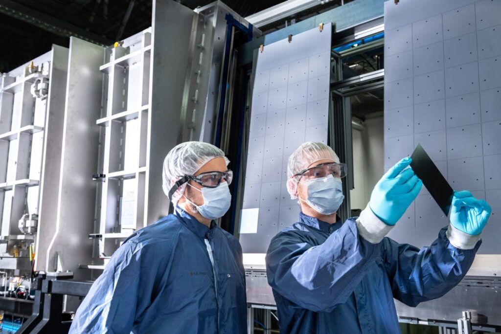
The company uses direct “gas-to-wafer” epitaxial technology to produce its solar wafers, where silicon crystal structures can be grown through chemical vapour deposition atop a crystal substrate. This contrasts with more common CZ wafers, which are made in a quartz crucible.
In a statement, NexWafe said these efficiency findings “validate NexWafe’s direct gas-to-wafer process as a seamless drop-in replacement for conventional CZ wafers”.
Furthermore, the company claims that the process offers “significant cost savings” compared with CZ production.
Epitaxy removes the need for wafer sawing, where a polysilicon ingot is cut into individual wafers. NexWafe CEO, Davor Sutija, told PV Tech: “When you don’t saw, you don’t have to do saw damage etch removal in the cell [production] process. So we reduce ordinary cell processing Opex by 5-7% just by skipping that step.”
He said that the process also avoids the material waste – or kerf – brought about by sawing polysilicon ingots. The company said: “While conventional CZ technology results in 50% material waste due to polysilicon losses, EpiNex reduces this waste to under 10%, primarily by eliminating wire saw kerf losses.”
Furthermore, Sutija said that the epitaxy process allows NexWafe to produce thinner and smoother wafers than its CZ competitors. These two physical characteristics could be significant for developing solar PV in space and the next generation of tandem solar technology.
Thinner (and thus lighter) wafers provide greater power-to-weight ratios, which is an important factor when building satellites for low-earth orbit. NexWafe said it has developed “ultra-thin 70μm cells” which would be well-suited to space applications.
More pressingly for much of the solar industry, the company said that its smoother products which have not been sawed could open the door to cheaper production of perovskite-silicon tandem solar products.
“Our epitaxial surfaces can have 10 nanometers roughness,” Sutija said, “And even the best-etched surface from CZ is 10 times rougher than that.
“Many new technologies, such as perovskite tandem, require you to put this polymeric film with perfect coverage on relatively large wafers,” he said. The company’s smoother products can allow that process to happen more easily and at greater scale, he claimed.
Diversifying the supply chain
Jonathan Pickering, VP for US business development at NexWafe, told PV Tech: “We’re in an era where companies are really pushing very hard on wafer thickness. CZ wafering technology was developed in the 1980s and 1990s and it’s just hitting a wall. It’s very difficult to make wafers any thinner – you can’t make the wire any thinner than 45 microns or it’s going to break, and you’re basically throwing away half of your material as kerf.
“The Chinese companies have done a wonderful job of scaling [CZ] technology,“ he said. “Driving down every last cent of cost, but it’s fundamentally expensive. You’re melting the silicon to 1410 degrees centigrade, then you’re sawing it up with wires and throwing half of it away. [Epitaxy] enables the industry to get on a whole new cost curve.”
China and Chinese companies dominate over 80% of the global solar supply chain – particularly in the costly and technical upstream portions like wafers.
NexWafe is one of a handful of companies – like glass manufacturer Corning and Korean-owned Hanwha Qcells – trying to bring wafer manufacturing capacity online in the west. The company is planning to build a 6GW wafer facility in the US and Sutija told us that it is also working with Indian conglomerate Reliance Industries on a pilot production line in India.
In a public statement, Sutija said: “Our technology creates an opportunity for regionally based manufacturers to compete with China…These latest results are transformative for photovoltaic wafer manufacturing.”
Specific technological innovations are often held up as the key to bringing large-scale solar manufacturing capacity outside of China. In the US, the upstream portions of the supply chain, like wafers and cells, have proved far more difficult to establish than module assembly plants. This is partly down to cost and time, but factors like energy demand, expertise and market saturation also play a part.
The US Department of Treasury recently introduced a 25% tax credit under the CHIPS Act for domestic solar ingot and wafer manufacturing operations. This followed repeated calls to provide subsidies for the domestic upstream industry to broaden the US’ solar supply security.
NexWafe is confident. Sutija said: “We’re poised for a very exciting two or three years.”
Pickering said: “We’re seeing tremendous interest from solar cell manufacturers, especially in the US and India, seeking a domestic supply of wafers. We’ve secured over 5GW in conditional supply agreements for mainstream solar markets and 250MW for ultra-thin cells for specialist applications.”


