Technical Papers

Premium
Market Watch, Photovoltaics International Papers
Predicting what will happen to the global PV market is very nearly an impossible task. Its underlying principles are very similar to the dozens of other electronics markets that IMS Research studies, but the key difference in the PV industry is the very close link to, and ultimate dependence on, government policy. In a few years’ time, the introduction, halting or change (or rumoured change) of a single government’s PV policy will have little effect on the global industry, and the huge swings in demand will be less common and less severe. The reasons for this are clear. First, because of geographic diversification in the industry, a single country will account for a smaller portion of the global total (unlike in 2011, when Germany and Italy accounted for more than half of global demand) and thus individual governments’ policy changes will have a smaller impact. Second, if system prices continue to drop rapidly (and IMS Research believes they will), a growing number of regions will achieve the ‘holy grail’ of grid parity and will thus no longer depend solely on government policy to drive their markets.
Premium
Materials, Photovoltaics International Papers
The purpose of this paper is to give an overview of the use and potential of diamond wire for the silicon-shaping process in the PV industry. The current market and future prospects for helping to meet the goals of 2020’s roadmap of thinner wafers and reduced $/W are described.
Premium
Photovoltaics International Papers, PV Modules
Crystalline silicon solar modules installed in the field are exposed to atmospheric conditions and experience stress, which induces a wear-out phenomenon in various parts of the modules and degrades performance over time. The performance eventually reaches a point where the output power falls below an acceptable level. Thermal cycling (TC) and damp heat (DH) are two important reliability tests for estimating infant failures related to materials and the manufacturing process, as well as providing the information on performance degradation with respect to time. In this study, modules composed of 156mm × 156mm multicrystalline silicon cells were subjected to TC and DH tests. By applying acceleration models, such as the Norris-Landzberg model for TC and the Hallberg-Peck model for DH, the minimum guaranteed life was calculated. The electrical and reliability results were interpreted and explained on the basis of the respective models.
Premium
Cell Processing, Photovoltaics International Papers
Coupled device and process simulation tools, collectively known as technology computer-aided design (TCAD), have been used in the integrated circuit industry for over 30 years. These tools allow researchers to quickly home in on optimized device designs and manufacturing processes with minimal experimental expenditures. The PV industry has been slower to adopt these tools, but is quickly developing competency in using them. This paper introduces a predictive defect engineering paradigm and simulation tool, while demonstrating its effectiveness at increasing the performance and throughput of current industrial processes. The impurity-to-efficiency (I2E) simulator is a coupled process and device simulation tool that links wafer material purity, processing parameters and cell design to device performance. The tool has been validated with experimental data and used successfully with partners in industry. The simulator has also been deployed in a free web-accessible applet, which is available for use by the industrial and academic communities.
Premium
Cell Processing, Photovoltaics International Papers
This paper presents examples of recent process developments at ECN in silicon solar cells on n-type monocrystalline base material. For all PV manufacturers, the challenge is to increase module efficiencies while maintaining low production cost. An effective way to move to higher and more stable efficiencies, using low-cost industrial-type processing, is n-type solar cell technology. The solar cell considered in this paper is the n-pasha cell – a bifacial solar cell with homogeneous diffusions and screen-printed metallization. The n-pasha cell is currently produced on an industrial scale by Yingli Solar; in 2011 a maximum solar cell conversion efficiency of 19.97% was obtained using this cell concept on 239cm2 n-type Cz at the ECN laboratory. The focus of the paper will be increasing efficiency by optimization of the cell process, in particular the front-side metallization, and by improvements to the rear-surface passivation. These two steps have contributed an increase in efficiency of 0.8%, allowing cell efficiencies of 20% to be reached.
Premium
Fab & Facilities, Photovoltaics International Papers
As a relative newcomer to the industrial world compared to more mature manufacturing sectors, the PV industry has not yet been subject to consistent environmental regulatory standards internationally. Like all industries that have preceded it, PV manufacturing is seeing its regulatory future evolve as PV producers migrate to different regions of the world. With this global expansion come significantly different levels of regulatory stringency, reflective of local conditions and cultures.
Premium
Photovoltaics International Papers, PV Modules
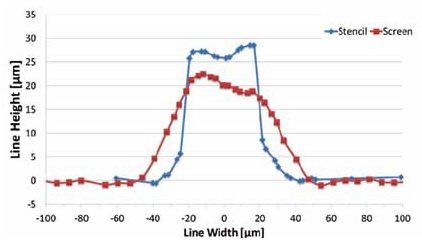
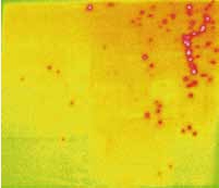
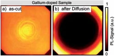
Non-destructive methods for measuring photovoltaic modules are discussed in this paper, with the aim of comparing different quality-assurance methods for different module technologies (e.g. crystalline and thin-film technologies: a-Si, CdTe, CIS). For a complete quality control of PV modules, a combination of fast and non-destructive methods was investigated. In particular, camera-based measurements, such as electroluminescence (EL) and infrared (IR) technologies, offer excellent possibilities for determining production failures or defects in solar modules, which cannot be detected by means of standard power measurements. These methods are applied effectively in quality control and development support, and EL is already an important characterization tool in industry and research. Most short circuits reduce the voltage in their surrounding area and appear dark in EL images. However, as this failure is not always critical and apparent, short circuits are only precisely identifiable in combination with IR measurements. Therefore, to quickly detect at high resolution the most common defects in a PV module, a combination of EL and IR measurements is advisable.
Premium
Materials, Photovoltaics International Papers
Most high-efficiency solar cells are fabricated from monocrystalline Czochralski silicon (Cz-Si) wafers because the material quality is higher than multicrystalline silicon (mc-Si) wafers. However, the material study presented in this paper reveals strong variations in the material quality of commercially available Cz-Si wafers, leading to a loss in solar cell efficiency of 4% absolute. The reason for this is the presence of defects, which appear as dark rings in photoluminescence (PL) images of the finished solar cells. It is shown that these efficiency-limiting defects originate from oxygen precipitation during emitter diffusion. It is demonstrated that an incoming inspection in the as-cut state is difficult, as strong ring structures in as-cut wafers turn out to originate most often from thermal donors. These are dissolved during high-temperature treatments and are therefore harmless, whereas moderate ring structures in the as-cut state may become severe. That is why critical wafers can be identified and sorted out reliably only after emitter diffusion, by using QSSPC-based lifetime measurements or PL imaging. The two-year statistics gathered from the research line at Fraunhofer ISE on the occurrence of ring defects in Cz-Si wafers indicate that ring defects are highly relevant in terms of material yield.
Premium
Photovoltaics International Papers, Thin Film
Advances in nanofabrication for enhancing the efficiency of optical devices, such as solar cells and photo-detectors, via nanostructuring have attracted a great deal of interest. A photoconversion strategy employing nanorods (NRs) has emerged as a powerful way of overcoming the limitations of planar wafer-based or thin-film solar cells. But there is also a broad spectrum of challenges to be tackled when it comes to putting into practice cost-effective NR solar cell concepts. ROD-SOL is a 10-partner, ‘nanotechnology for energy’ project with end-users, equipment manufacturers and institutes from six countries forming the consortium. The aim of the project is to provide the photovoltaic market with a highly efficient (> 10%), potentially low-cost, thin-film solar cell concept on glass, based on silicon nanorods. This paper presents the project’s achievements and discusses what the future might hold for nanotech-based solar energy production.
Premium
Photovoltaics International Papers, Thin Film
Today, crystalline-Si photovoltaics (PV) dominate the market, accounting for more than 85% of market share in 2010. A large scientific community made up of academic as well as industrial stakeholders strives to find solutions to improve device efficiencies and to drive down costs. One of the important cost elements of a module is the c-Si wafer itself. This paper discusses the fabrication of a carpet of c-Si foils on glass, either by layer transfer of an epitaxially-grown layer or by bonding of a very thin wafer, and processing this c-Si thin-foil device into a photovoltaic module. This could constitute an advantageous meet-in-the-middle strategy that benefits not only from c-Si material quality but also from thin-film processing developments.

Subscribe to Newsletter

Upcoming Events

Solar Media Events
June 17, 2025
Napa, USA
Upcoming Webinars
June 30, 2025
10am PST / 6pm BST
Solar Media Events
July 1, 2025
London, UK
Solar Media Events
July 1, 2025
London, UK
Solar Media Events
September 16, 2025
Athens, Greece