Organic/inorganic lead halide perovskite solar cells (PSCs) have received global attention because of their excellent photovoltaic performance and ease of fabrication.
PSC’s have reached over 24% power conversion efficiency demonstrating that the lead halide perovskites are the most promising class of materials for next-generation thin-film photovoltaics. The unprecedented increase in the device performance from 3.8% to 24% in less than 10 years is mostly due to compositional engineering of mixed cations, and anions, as well as improved processing protocols has made PSC the fastest development of a new material in the PV field.
Try Premium for just $1
- Full premium access for the first month at only $1
- Converts to an annual rate after 30 days unless cancelled
- Cancel anytime during the trial period
Premium Benefits
- Expert industry analysis and interviews
- Digital access to PV Tech Power journal
- Exclusive event discounts
Or get the full Premium subscription right away
Or continue reading this article for free
Though the efficiencies on lab scale are staggering, the full potential of this burgeoning technology cannot be realized without addressing the following challenges: fighting the degradation of the material is the highest focus for the moment and has several fronts for improvements including within larger scale cells or modules.
The other main challenge of the new class of material is the toxicity risks due to the presence of lead. The research community is actively working on the mitigation and reduction of the associated risks. The exceptional properties of this material combined alongside its inherent relative lower costs have already triggered the interests of industries and start-up worldwide while on a European regional level, EPKI for European Perovskite Initiative was formed gathering all the significant players in the field.
Introduction
Calcium titanate Perovskite (ABX3) is a class of semiconductors discovered in the middle of the 19th century and named after Russian mineralogist Lev Perovski. This ABX3 crystal structure was first studied as a PV absorber material in 2009 by Tsutomu Miyasaka et al., by mixing lead bromide and methylammonium bromide and obtaining an instant crystallization through a spin coating process.
This first PSC generated a 3.8 % Power Conversion Efficiency (PCE), and was based on a mesoporous TiO2 anode. At that time, the device would not last more than a few seconds since the electrolyte dissolved the perovskite crystals quasi instantly. Later helped by Oxford University, the recipe was tuned with the addition of an organic hole conductor material into the device that conferred enhanced stability and efficiencies at around 10%. Then came the discovery that perovskite is not only a light absorber but also as an electron and hole conductor itself changing the vision of the research community.
PSC typically consists of a conducting glass (or polymer) deposition, an electron extraction layer typically TiO2 or SnO2, then comes the essential active-perovskite material and on top a hole transporting material and electrodes usually gold, terminate the stack (The inverted configuration being also an option).
One of the core quality of the Perovskite is the tuneability of its bandgap from 1.15 to 3.06 eV depending on the interchange and mix of different “A” cations such as rubidium (Rb) cesium (Cs), methylammonium (MA) or formamidinium (FA) as well as the associated metals “M” or halides “X”: The tuning options are endless. Large bandgaps perovskite materials are used for non-PV applications such as photodetectors, LED, sensing and X-ray detection, when photovoltaic requires a typical 1,2 to 1,4 eV.
PSC’s are being developed as both single junction, and multiple layers of perovskite (multiple junctions) as well as transparent solar cells and the promising tandem configuration such as c-Si/perovskite and CIGS/ perovskite. At a later stage, the potential of concentrated perovskite could be a path towards higher efficiencies.
The interest of the research community literally skyrocketed in the past 10 years and laboratories worldwide were racing for the highest conversion efficiency which in early 2019 reached an astonishing 24.2% in a single-junction architecture.
Further, the combination of semi-transparent / Perovskite layers on top of other PV materials, already resulted in a 28% c-Si/Pk, a 25.6% CIGS/ Pk and a 25% Pk/Pk tandem efficiency, all above record cell efficiencies of the bottom PV cell.
Scaling-up to larger areas
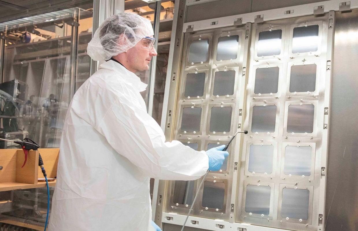
Whilst laboratory scale PSC’s are the size of a coin and are breaking efficiencies records, one of the challenges remains in up-scaling to larger areas. Device architecture as well as the choice of the sandwiching contacting materials (hole transport layer and electron transport layer – ETL and HTL respectively) play a major role for upscaling to modules and panels.
Highly efficient Perovskite Solar Modules (PSMs) or mini-modules in the direct n-i-p structure are reported in the literature with a PCE of 16% on 10cm2 and 12.6% on 50cm2. Besides the intrinsic losses due to size effects, it must be clear that the process transfer from single solar cells to large area arrays of devices is not trivial and since it is about controlling the nucleation and growth of perovskite grains/ crystals uniformly on a large area.
Important to mention here that most of the record devices were made with solvent quenching which is not scalable. Intrinsically low cost, versatile chemical methods for industrial scale production which fully avoid solvent residues and collateral effects are yet to be developed. In parallel to chemical methods, physical approaches are being explored, since they would intrinsically guarantee low-contaminant level, almost zero waste and high production throughput for reproducible and reliable processes. In addition, physical processing steps would be more likely integrated in established flow-charts for production of inorganic solar cells or in view of possible business conversion of existing semiconductor industries to perovskite solar cell manufacturing.
In this aspect, automatic processes combining superior material deposition control and high throughput are to be successfully applied for getting the expected low cost PSMs. Therefore, significant efforts have been spent to boost up large-area methodologies such as: ink-jet, screen-printing, spray-pyrolysis and doctor-blade coating or roll to roll printing in combination with ultrasonic spray coating or vapor deposition. It is fair to admit that many of these deposition methods have already been developed and tested more generally for thin film PV.
It is however acknowledged largely that Perovskite-based PV is very promising in terms of cost efficiency: The advantages of perovskites PV with respect to silicon PV stands on their easy and low cost synthesis, cheap precursors, low-temperature solution processing and possibly high throughput manufacturing and the cells are also displaying rather high efficiencies, great low light performance, as well as low weight (ideal on foils). This theoretical cost advantage is essential for its future success but equally important will be the long term stability of its performance to guaranty the best LCoE.
This is an extract from a technical paper published on PV Tech. The full paper is free to view, and can be found here.
Author biographies
Louis Huber
Consultant and Business Developer with 12 years’ experience in PV mainly on installation, EPC contracts, PV modules sales and sourcing, European BD and collaborations. He is now working independently from Brussels and Paris within the EPKI program, as promoter and mediator between Research, Industry and political arena.
Alessandra Alberti
Ph.D. cum laude in Physics and Researcher at Institute for Microelectronics and Microsystems of the National Research Council of Italy in Catania from January 2001. Expert in physical deposition methods (sputtering and sublimation) and High-Resolution X-Ray Diffraction/Reflection. Long-lasting collaborations with the prof. T.Miyasaka’s team. Author of >100 JCR papers and Italian/USA patents.
Ioannis Deretzis
Doctor and Researcher at the institute of Microelectronics and Microsystems in Catania, Italy. He is working on various fields of computational materials science and theoretical solid-state physics. His current research interests focus on low-dimensional materials and hybrid perovskites.
Professor Nazeeruddin
Current research at EPFL focuses on Perovskite Solar Cells and Light-emitting diodes. He has published more than 630 peer-reviewed papers, ten book chapters, and inventor/co-inventor of over 75 patents.He is elected to the European Academy of Sciences (EURASC), and Fellow of The Royal Society of Chemistry.According to ISI listing, he is one of the most cited chemists in 2014, 2015, 2016, 2017 and 2018, and one of the 20 scientists identified by Thomson Reuters as The World Most Influential Scientific Minds.


