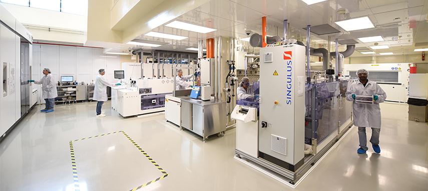
Researchers at the Solar Energy Research Institute of Singapore (SERIS) at the National University of Singapore (NUS) have announced the development of a significantly low-cost technique to texture nanoscale features on multicrystalline silicon (mc-Si) wafers after diamond-wire wafer cutting.
SERIS noted that the wide adoption of mc-Si wafer diamond-wire wafer cutting has been limited by existing etching processes being deemed expensive and degrade conversion efficiencies. Reactive ion etching (RIE) is not deemed a low-cost process, while metal-catalysed chemical etching (MCCE) techniques can add metallic particle contaminants.
Try Premium for just $1
- Full premium access for the first month at only $1
- Converts to an annual rate after 30 days unless cancelled
- Cancel anytime during the trial period
Premium Benefits
- Expert industry analysis and interviews
- Digital access to PV Tech Power journal
- Exclusive event discounts
Or get the full Premium subscription right away
Or continue reading this article for free
“Our technology is simpler, cheaper, metal-free and can achieve cell efficiencies of more than 20%. For these reasons, I strongly believe that our technology can become a mainstream texturing technology used by mc-Si solar cell manufacturers”, said Dr Huang Ying, the lead inventor of SERIS’ DWS Wafer Texturing Technology.
The SERIS wet-chemical technique uses proprietary chemicals to etch the mc-Si wafer surface that creates nanoscale features with dimensions smaller than the incident light wavelength, which enhance light capture with the potential for mc-Si solar cells achieving conversion efficiencies of 20%.
SERIS noted that such cell conversion efficiencies are about 0.5% (absolute) higher than those currently mass produced by leading PV manufacturers.
Dr Joel Li, Head of the Multicrystalline Silicon Wafer Solar Cell Group at SERIS added, “We have addressed a long-standing challenge faced by the PV industry with our technology, and it has been proven to be an effective method for texturing DWS multicrystalline silicon wafers at low cost. The PV industry can leverage our technology to enable the switch from slurry-cut to cheaper DWS multicrystalline silicon wafers, which are 5-15% cheaper. For a gigawatt factory, this translates to cost savings in the order of US$10 million per year. In a cost-sensitive industry like PV, this level of cost savings is highly attractive”, said Dr Joel Li, Head of the Multicrystalline Silicon Wafer Solar Cell Group at SERIS.
“This low-cost texturing approach holds immense potential in facilitating substantial cost reduction for the PV industry, and it has already been recognised by several tier-1 manufacturers. SERIS plans to license the technology to interested manufacturers and work closely with them to implement and scale up the texturing process on their production lines. As the PV industry experiences a major shift from slurry-cut to DWS mc-Si wafers this year, we believe that this novel technology developed by SERIS will become a mainstream texturing technology for DWS mc-Si wafers”, said SERIS CEO Prof Armin Aberle.
")


