PV Tech and Kontron AIS are co-hosting a webinar exploring how new MES software can optimise PV manufacturing even as new technologies and manufacturing methods are adopted. Registration for the webinar, which takes place on 17 May 2022, can be found here.
Product Outline
Try Premium for just $1
- Full premium access for the first month at only $1
- Converts to an annual rate after 30 days unless cancelled
- Cancel anytime during the trial period
Premium Benefits
- Expert industry analysis and interviews
- Digital access to PV Tech Power journal
- Exclusive event discounts
Or get the full Premium subscription right away
Or continue reading this article for free
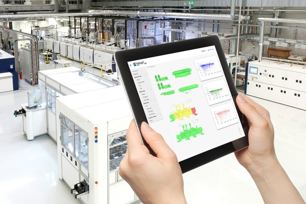
Kontron AIS is supporting PV manufacturers with a standardised Manufacturing Execution System (MES) for production control, material track and trace and equipment performance tracking, covering all processes from crystal growing over wafer and solar cell production to module assembly. The MES has proven its ability to secure quality, optimise manufacturing processes and save costs across the PV industry for over 15 years.
Problem
The challenge is to integrate an MES system which allows a PV manufacturer to closely control every step of the value chain. This requires a full vertically integration of manufacturing processes such as crystal growing, wafering, solar cell processing and solar module assembly.
Manufacturers install such MES to achieve traceability for all products from raw silicon through crystal, ingot, wafer, solar cell up to the finished solar module. The goal is to keep track of all transactions and operations to determine precisely what was done to the product, when was it processed, at which equipment and under which conditions.
Solution
Process and equipment data acquisition is conducted using various standard compliant equipment interfaces like SECS/GEM, PV2, XML, OPC-UA and S7. These interfaces are used to reliably communicate the equipment state, material movement, process parameter and equipment data.
Material and carrier interlock commands are used to prevent material mishandling and to enforce the orderly execution of the steps in work plans. Product yield is improved, and scrap reduced by enforcing the execution of the work plan and tightly controlling and monitoring manual and automatic material processing.
Material tracking and tracing data ensures besides correct inventory data and end-to-end backward and forward genealogy. Backward tracking starts from the finished solar module relating it back to solar cells, wafers, ingot, crystal, raw silicon, and related consumables to build a module. Forward tracking starts from raw silicon tracking it to all the finished solar modules that were produced using a certain silicon lot.
Real-time connection to the ERP system is used to continuously exchange master data, work orders, production progress and quality information to keep track of semi-finished and finished product inventory and the associated consumption of raw material and consumables.
The acquired equipment data is used to calculate KPIs like OEE. This allows closely monitoring and improving equipment performance.
Applications
Crystal growing (e.g. Czochralski process) including silicon commissioning with recipe handling, different raw silicon types, dopant, seeds, crucible, hot zone part tracking, re-charge scenarios, multiple crystal unloads, scrap handling, manual data collection, yield and inventory tracking, cropping, automatic and manual lifetime, resistivity measurement, tracking of cropped parts and scrap recycling of silicon including etching, sorting.
Wafering processes including inspection, mounting, squaring, chamfering, slicing, singulation, pre- and final cleaning, classification and sorting.
Solar cell processing, batch and single wafer processes including texturing, diffusion, CVD, PVD, PECVD, printing, classification and sorting, transport system tracking, virtual wafer tracking and consumable tracking.
Solar module assembly processes including glass washing, stringing, matrix layup, inspection and rework, lamination, framing, junction box mount, flashing and palletizing.
Platform
Integrates seamlessly in local IT infrastructure or public cloud environments.
Availability
Available worldwide now.