The rise of tunnel oxide passivated contact (TOPCon) technology has been impressive. As of the start of 2026, it accounts for almost 85% of global production, while mono PERC has declined to less than 5%, according to market analysts CRU. N-type TOPCon offers clear advantages over p-type PERC, including higher conversion efficiency, a better temperature coefficient and superior resistance to degradation. CRU’s Solar Module Tracker reports that leading TOPCon module efficiencies now exceed 24.5%, with median module efficiencies coming in at 23%.
The transition from PERC to TOPCon has largely been an evolution rather than a revolution for manufacturers. Many existing PERC production lines were able to be upgraded to TOPCon, and even when new lines were built, the technology did not require unfamiliar equipment or production processes.
Try Premium for just $1
- Full premium access for the first month at only $1
- Converts to an annual rate after 30 days unless cancelled
- Cancel anytime during the trial period
Premium Benefits
- Expert industry analysis and interviews
- Digital access to PV Tech Power journal
- Exclusive event discounts
Or get the full Premium subscription right away
Or continue reading this article for free
Another key advantage was that the majority of Chinese cell manufacturers adopted TOPCon on a similar timeline. Broadly speaking, this meant that the roughly 500GW of PERC production capacity available in 2020 was first replaced and then expanded with the addition of around 1TW of TOPCon capacity. This large-scale shift to TOPCon enabled the Chinese supply chain – including both production equipment and consumables – to scale alongside cell and module manufacturers.
Status update: current TOPCon production in China
In 2026, market conditions for new PV production facilities are well understood. With nameplate manufacturing capacity far exceeding market demand, there is little interest in establishing new production lines in the PV manufacturing powerhouse of China.
Outside of China, however, a different dynamic is emerging. Driven by a growing focus on local value creation in PV production, a more geographically diverse manufacturing landscape is taking shape. In countries such as India, the United States and Türkiye, PV cell production facilities have already been established, and an encouraging new wave of production is taking root.
In its latest Energy Transition Investment Trends report, BloombergNEF found that while China remains the dominant solar manufacturer globally, its share of annual investment in new manufacturing capacity is gradually declining. This shift highlights the significant production investment occurring outside of China, particularly in the United States and India, reports BloombergNEF, where efforts to onshore solar and battery supply chains are accelerating.
Yet the conditions for TOPCon production outside China are markedly different. Supply chains for key production processes and consumables are often less developed, and cost structures that are competitive in China can be prohibitively expensive elsewhere. While these factors present challenges, they also create opportunities. New TOPCon producers in emerging manufacturing hubs can adopt high-volume, scalable production processes that deliver advantages in both capex and opex, while also providing a foundation for future upgrades to tandem cell architectures.
TOPCon production processes and volatile, toxic gases
At present, TOPCon producers in China primarily use either low-pressure chemical vapour Deposition (LPCVD) or plasma-enhanced chemical vapour deposition (PECVD) equipment for several key process steps, including those that give the technology its name (see cell diagram, Figure 1).
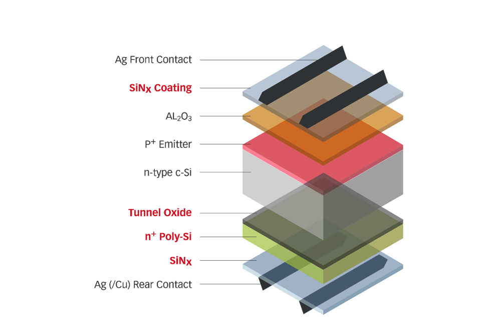
On the rear side of the cell, LPCVD or PECVD is commonly used to deposit both the tunnel oxide (TO) layer and the highly doped n-type silicon layer in Chinese cell fabs. The TO layer is extremely thin, typically 1.5-2.0nm, while the amorphous silicon (a-Si) layer is around 50-100nm and is usually phosphorus-doped. There are some manufacturing lines that use a thermal process for TO deposition, which requires additional equipment.
Within this rear-side process flow for TOPCon cells, phosphine (PH₃) gas is frequently used for the phosphorus doping of the a-Si layer. Phosphine is highly toxic and volatile, and can be pyrophoric, meaning it can self-ignite in air. Therefore, its use requires a comprehensive range of safety measures, including continuous air monitoring, highly secure storage, gas evacuation systems, robust ventilation, dedicated safety infrastructure such as gas bunkers and extensive use of personal protective equipment (PPE). This additional complexity can considerably increase fab capex, especially in regions where the infrastructure for handling hazardous gases is less established.
Silane (SiH₄) gas is also widely used in CVD processes for a-Si deposition. Like phosphine, silane is pyrophoric and can combust when exposed to air, creating an immediate and often invisible fire risk. As a result, its use requires specialised high-pressure piping and stringent fire safety precautions. The Chinese PV industry has developed extensive expertise in handling these hazardous gases and has built a mature supply chain for both the gases themselves and the hardware required for their safe handling. This is often not the case outside China. For example, VON ARDENNE engineers have observed that silane gas costs can be multiple times higher in Türkiye than in China. In addition, facility-related costs – such as the gas storage, piping and required disposal systems – can significantly increase capex in countries like the United States, while also delaying permitting timelines for new facilities or fab upgrades.
Complex workflows, sprawling fabs and automation requirements
When CVD processes are used for rear-side TO and a-Si deposition, additional processing steps are necessary. CVD typically results in some coating on the wafer edges and frontside, which must then be removed. Unlike heterojunction, TOPCon is not a symmetrical cell architecture, and it is critical that no n-type-doped silicon remains on the front side of the cell, where a boron-doped emitter is required. As a result, when CVD is used for rear-side coating, additional wet chemistry steps are needed to remove any unwanted edge or front-side deposition.
To passivate the front side of the cell, an aluminium oxide (Al₂O₃) layer is applied, for which atomic layer deposition (ALD) processes are standard. On top of this layer, and also on the rear side of the cell, an anti-reflective coating, commonly silicon nitride (SiN), must be added. This coating is what gives TOPCon cells their characteristic blue colour on both the front and rear side, despite their asymmetric architecture.
In China, SiN deposition is typically performed using PECVD. This is usually carried out in two separate steps on two different PECVD tools: first for the front side and then for the rear. Automated handling equipment is used to load, unload and transport cells during both coating steps and between deposition tools.
The PVD alternative for scale, safety, and supply chain
In China, it is abundantly clear that the PV industry has become highly proficient at deploying CVD processes for TOPCon production, achieving competitive cost and performance benchmarks. However, there are alternative approaches. Physical vapour deposition (PVD) is a proven and mature technology in PV manufacturing that avoids many of the safety and supply chain challenges associated with toxic and flammable process gases.
Whereas CVD processes rely on hazardous and volatile gases, PVD sputtering uses solid-state targets. In terms of the deposition process, rear-side TO and silicon layers can be applied using PVD in an inherently single-sided process, avoiding edge and front-side contamination.
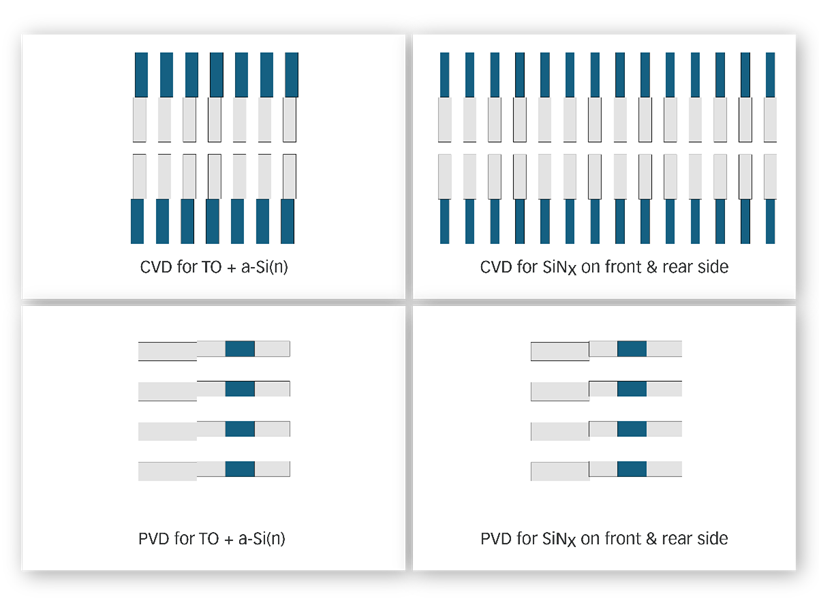
PVD also offers advantages in scalability and throughput due to its inline processing capability. Continuous 24/7 coating of both front- and rear-side SiN layers or TO and a-Si deposition on the rear side can be performed within a single tool, eliminating the need for manual or automated loading and unloading across multiple CVD systems. An example of such a tool is VON ARDENNE’s GIGANOVA platform, which can be supplied with either a single-sided or double-sided coating capability.
To illustrate the fab footprint advantages double-sided coating delivers, let’s compare typical PVD and CVD equipment requirements for a high-volume TOPCon cell line. A 4-5GW TOPCon cell line requires four PVD tools for rear-side TO and a-Si deposition, plus another four tools for front and rear-side SiN deposition (see Figure 2). By contrast, CVD-based process flows can require up to 42 individual pieces of equipment.
Performance advantage and tandem development
From a performance standpoint, PVD demonstrably achieves the same high efficiency levels as established CVD-based TOPCon production. There is no indication of any performance disadvantage when implementing PVD at an industrial scale.
Research by the Fraunhofer Institute for Solar Energy Systems ISE shows that PVD-deposited silicon nitride (SiN) layers offer excellent thickness and refractive index uniformity. This superior homogeneity improves the optical consistency of the anti-reflective coating across the wafer surface and supports stable passivation and contact properties. Any measured differences in cell efficiency are typically small and mainly attributable to these optical effects rather than to fundamental electrical advantages.
For PV cell manufacturers, the next major question is no longer only focused on scaling TOPCon, but what comes next. Tandem cell structures are widely seen as the most likely path to the next major step-change in performance needed for long-term competitiveness.
PVD tools are already being widely used by developers of perovskite tandem technologies. For TOPCon manufacturers seeking to establish production lines that can be upgraded to tandem cells, this offers a clear advantage. On an existing TOPCon line, the frontside SiN deposition chambers in a PVD system can be repurposed for transparent conductive oxide (TCO) and electron transport layer (ETL) deposition. In practice, this means an existing PVD tool used for TOPCon can be adapted for tandem production by changing the frontside sputter targets – something that is not possible with PECVD systems.
Looking towards the performance potential of TOPCon-perovskite tandem devices, Trina Solar announced in February 2026 a full-size module efficiency of 32.6%, delivering 886W on a 3.1m² module format. Trina collaborates with European-based perovskite-tandem technology developer Oxford PV. This exciting milestone suggests that previously assumed performance limits for PV modules are now being surpassed.
TOPCon producers outside of China face a challenging marketplace. And while China has mastered the large-scale industrialisation of crystalline silicon through highly standardised production workflows, the next wave of TOPCon production beyond the borders of the manufacturing giant will demand a new, more strategic approach. In addition to energy conversion efficiency, other factors will also play a crucial role in technology selection. Considerations such as safety, infrastructure requirements, equipment footprint, scalability, tandem compatibility and intellectual property (IP) protection remain the more compelling drivers in choosing the right production technology.
Dr Sebastian Gatz is vice president, renewable energies & strategic partnerships, at VON ARDENNE.


")


