This blog contains the concluding part of my Tales from Taiwan feature, with the first blog – Tales from Taiwan Part 1: more capacity comes online, but not in Taiwan – appearing on PV-Tech earlier this week.
The topics, themes and discussion were stimulated by my travels to Taiwan last week, overlapping with the PV Taiwan exhibition, and meetings with almost every equipment and materials supplier to the industry.
Unlock unlimited access for 12 whole months of distinctive global analysis
Photovoltaics International is now included.
- Regular insight and analysis of the industry’s biggest developments
- In-depth interviews with the industry’s leading figures
- Unlimited digital access to the PV Tech Power journal catalogue
- Unlimited digital access to the Photovoltaics International journal catalogue
- Access to more than 1,000 technical papers
- Discounts on Solar Media’s portfolio of events, in-person and virtual
The blog is divided into two parts. The first part looked at some of the new capacity still coming online, and outlined what to expect in 2017 from technology upgrades and process improvements.
The second part of the blog here discusses the wider implications of having two integrated c-Si manufacturers, collectively driving the industry in a way we have not seen before.
Yet more pressure on n-type, with LONGi calling the shots
I finished the first blog by noting that the two key technology upgrade steps in 2017 are likely to come from p-type mono cells (PERC) and p-type multi wafer/cells (diamond wire and new texturization).
If we decide to look at these together, then we can see quickly that 2017 could be more a shift to further increase the competitiveness of p-type cells/modules (both mono and multi), compared to all n-type variants on the market today (HJT, IBC and n-PERT).
Clearly, this puts all n-type companies under pressure to work out how to substantially decrease their wafer ASPs and cell production costs, bearing in mind that n-type ingot pulling and wafer slicing are steps that reside with (far less aggressive and capacity-constrained) third-party suppliers that are basically not married to end-market module supply drivers.
Or put another way: n-type is still fragmented, and it is hard to see anyone stepping up to change things radically in the near term.
Ultimately, it is becoming clearer here also just how important LONGi (and LERRI Solar) could be in the mix of c-Si supply as we enter 2018. And we are moving to the stage that n-type market share from the entire n-type cell community could be dictated by if, or when, LONGi change ingot pulling from p-type to n-type wafer supply.
LONGi n-type shift needs to help LERRI Solar, not others
As far as I see it, LONGi really does not have any motivation from a competitive standpoint to do any shift in 2017, as this would simply empower LERRI Solar’s competitors in the market that are currently running n-type cell and module lines. Especially at the most important period in LERRI Solar’s business plan that is driven by getting the company on the global stage as a leading module supplier to the industry both inside and outside China. Enabling for example SolarCity to have a low cost wafer supply to Buffalo is not exactly going to help LERRI Solar gain market-share in the US, and the same could be said for Panasonic, SolarCity, SunPower and LG Electronics.
Surely, if or when LONGi does any shift from p to n-type ingot pulling, this will be at the point when it is most favourable to LERRI Solar’s market competitiveness, not a day before. Otherwise, the company may run the risk of grabbing short-term revenue gains from its wafer business (LONGi) at the expense of substantially greater long-term profits from module activities (LERRI Solar and downstream projects business).
First signs of what vertically integrated really means for solar
Controlling the technology choice of your competitors?
What a strong position to be in, and one that is almost unique today in the solar industry.
I believe we should be potentially viewing LONGi/LERRI as not just a company that is rapidly approaching the Silicon Module Super League (SMSL) status of Canadian Solar, JA Solar, JinkoSolar, Hanwha Q CELLS and Trina Solar, but is actually much more important than any of these competitors in being able to reshape the manufacturing landscape to its benefit.
As our in-house research team did the finishing touches on the PV Manufacturing & Technology Quarterly report, released last week, the full implications of LONGi/LERRI’s status in the solar industry were just starting to emerge. After last week’s meetings in Taipei, we were able to sanity check some of these. And the above n-type versus p-type dynamic was one of the issues that seems to me to be potentially a game-changer and not directly obvious from a basic model and forecast for LONGi/LERRI Solar.
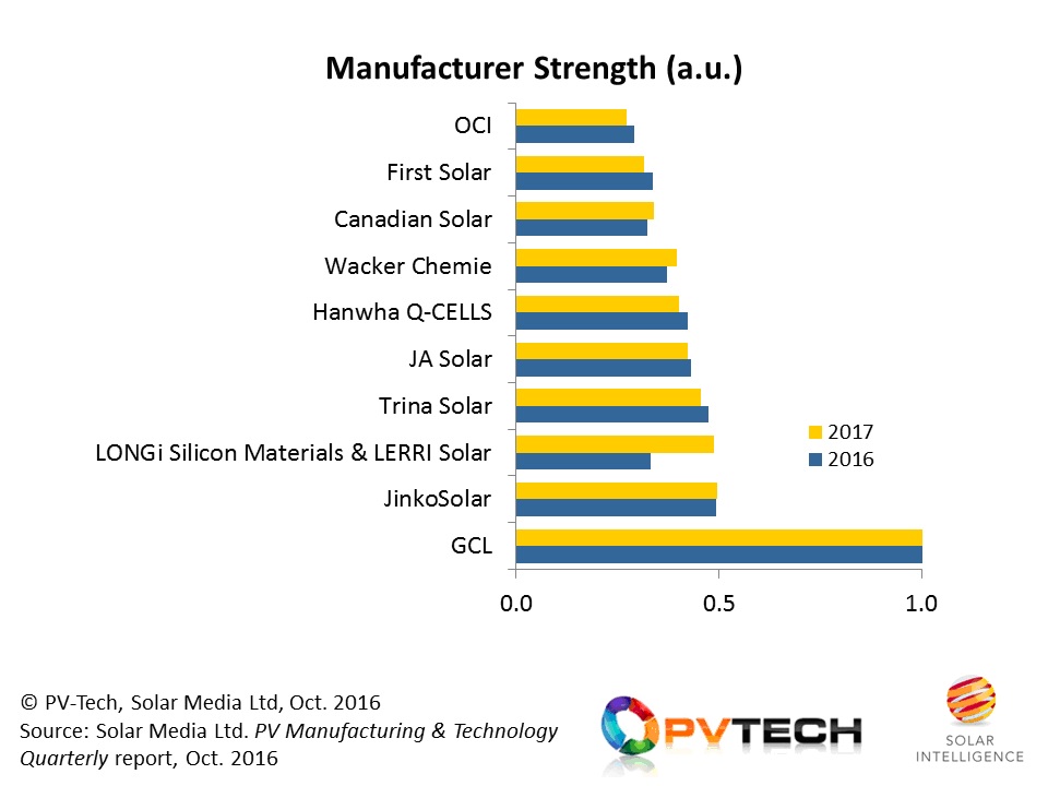
The graphic below is an updated visual on our recently developed methodology we devised to benchmark every PV manufacturer across the poly to module and thin-film value-chains. It gives some colour on the increased status of LONGi in the PV industry going into 2017, in addition to clarifying the continued power of the other company ring-fenced in this blog – GCL.
Diamond wire saws: the only route for p-multi to go next year?
Moving swiftly now to GCL (viewed as a single entity from poly-to-module and projects), it is still the wafer part of GCL Poly that is considered to be the most critical in terms of 2017. And this takes us neatly into the p-multi side of the debate.
Having had the luxury of a significant pricing advantage for several years and seeing constant efficiency enhancements, p-type multi has dominated the industry, and GCL Poly has been fully in control of this.
But two things have happened in the past 12 months: LONGi scaled p-mono wafer supply, very close to p-multi price points; and PERC became the go-to upgrade path on p-mono cells that is retaining approximately a 5% ASP premium on cells produced using a full aluminum back surface field.
Basically, if p-mono wafers get within a few percentage points of p-multi wafers, the entire industry flips to p-mono; it is that simple, as long as there is enough supply (which there isn’t now!).
So, if you are a champion of p-multi wafers (and cells), which is the mainstay of manufacturers in Taiwan, where do you take p-multi?
The do-nothing option is ugly. The only route here is to see your p-multi wafer ASPs collapsing relative to p-mono – exactly what happened when p-mono wafer ASPs got close a few months back.
The more sensible approach is to improve wafer performance more, actively take more cost out the manufacturing, and enable your customers (p-multi cell makers) to make changes at the cell stage. And as such, we have the basis behind the current drive for what is called ‘black silicon’.
For starters, let’s get one thing straight. We are not talking about black silicon in the true sense of the word. Black silicon is a different beast. And it is best to talk about what is actually the deal here: moving multi wafer slicing to using diamond wire saws (DWS).
Very quickly; DWS saves you about 10% on costs, almost regardless of the other costs, because DWS basically translates to getting 10% more wafers out of production. The use of DWS is okay for mono or multi, but so far has only been applied to p-mono.
The stumbling block for using DWS for p-multi wafers is at the cell stage: existing texturization methods on p-multi (almost all using wet benches) are not compatible with the different surface finish from the DWS process, requiring a greater level of surface texturization that can be met with either dry etching (such as RIE) or metal-assisted chemical etching.
Therefore, for DWS to gain traction on p-multi, cell changes need to be synched to wafer changes, and vice-versa. And even if that does happen on the occasional line here or there, it basically needs GCL to be in the driving seat to have any chance of coming to fruition across the p-type industry as a whole.
It’s not my problem
Where make the changes though? Should wafer manufacturing include what is currently front-end cell texturization? Of should cell makers do all the changes themselves, as is currently the norm?
With this in mind, one of the few (if not the only) wafer manufacturer currently taking the pole position is Gigastorage Corporation. The picture below, taken at PV Taiwan, shows two different 60-cell modules using p-multi cells made with DWS multi wafers. The two different modules are using each of the texturization methods under consideration. (It helps if your company makes the diamond wires also.) What is different here is that Gigastorage is supplying the wafers with the texturization done, therefore allowing cell makers to avoid making this switch. This may end up the de-facto route for DWS/black-silicon.
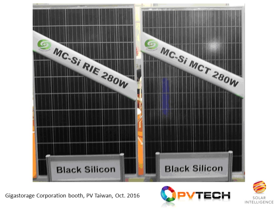
Actually, as a glimpse of what 2018 may look like, the modules shown in the picture above are actually p-multi PERC, with Taiwan having possibly the number-four ranked p-type multi PERC cell producer right now. 60-cell p-multi modules at 280-290W is a mouth-watering prospect, if this is to become the industry norm during 1H’18 from the multi segment, using wafers that have an instant 10-15% cost saving.
It is this level of technology progress that is almost certainly needed from p-type multi to retain market competitiveness in 2017 and 2018, without having to resort to price as the only option.
And what if they helped each other?
It is just not clear what the others should do, if we end up going into 2018 with GCL and LONGi offering p-mono and p-multi wafers at price and performance points that none of the others can come close to.
We even need to look at the other SMSL players that have tried to bolster in-house wafer/cell capacity in recent years, and whether they (as at best 1GW-level wafers players) can justify the case for in-house wafering.
While I hate to conform to headline grabbing prophesy – and the use of the dreaded word ‘consolidation’ – maybe one can make a strong case for consolidation across p-type wafering capacity in China with many of GCL’s existing cell customers coming under the ownership of GCL. It is not a difficult one to imagine happening, as much of this capacity was initiated with what seemed before like some kind of unofficial blessing of GCL-Poly itself.
Now, if you just happened to be a conspiracy theory market researcher, then could the best result for both LONGi and GCL not be achieved through some kind of formal or informal strategy alignment, the end goal being for each of them to own 50% of the global solar industry wafer supply, split evenly across mono and multi?
Or, if price fixing was above board and legal, then you could make the case for having a dual p-type mono/multi wafer plan that saw each ASP trending downwards as fast as possible, significantly improving performance, and feeding directly into the black-silicon and PERC cell roadmaps of 2017; as long as the delta between mono and multi hovers in the 10-15% range. If LONGi and GCL was a single company (and I was its CEO), I may be inclined to push that option in 2017 to rid the industry of as much competition as possible.
Maybe in practice, so long as neither infringes on the value-added of the other, the end result will be the same: a solar industry with two wafer power-houses, in control of >95% wafer revenues.
Vertical integration at last
For as long as solar PV has existed, manufacturers have toyed with the option of being vertically-integrated, with full control of costs and technology across the entire value-chain. Many have tried: nobody has managed it. For some, it has been the catalyst in propelling the company to imminent insolvency and years in zombie-world.
Lots of reasons have been given over the years about why vertical integration has not worked, and most of them tend to be wrong, and are mainly a by-product of what I think is the real reason, as follows:
For vertical integration to work in the solar industry – and to be successful almost regardless of what is happening elsewhere across supply, demand and pricing – two conditions need to be in place:
1. Capacity through the value-chain needs to be significantly higher than anyone else. So, in today’s solar lanscape, this probably means being above 10GW, but probably 20GW is a better number.
2. Performance and cost at any stage (ingot, cell, etc.) has to be industry-leading, as if viewed in isolation as a stand-alone business. You can’t hide mediocrity, just because you have capacity levels in place or a vertical strategy.
And if you simply apply this logic to the previous efforts of companies to be vertically-integrated, you can see very quickly that nobody came anywhere close to these, and as a result, the companies were not shielded from any market tremors and generally fell before any first hurdle was even reached.
So, while we are not anywhere close to these conditions being met for LONGi or GCL by the end of 2017, we could be seeing the first signs of what may unfold sometime in the future, with even the current polysilicon cartel being disrupted by LONGi taking the move upstream to polysilicon. (One could make the case to some extent for acquisition here by LONGi, with Chinese competitors of GCL or overseas options like Tokuyama candidates that could be in the firing line.)
One can get into speculation galore, so let’s get back to what we know today and wrap up on the learnings out of Taiwan.
A final word on Taiwan
All said and done, the PV community in Taiwan remains by far the most knowledgeable on trends and challenges relating to c-Si wafer and cell manufacturing. And while the country’s legacy USP – making cells – may be going through a prolonged period of stagnation as the fall guy in the ongoing retaliatory trade ping-pong that is China-versus-the-US-and-Europe, the fact that all the Taiwan manufacturers are part of a harmonious community that does not employ competitor-annihilation tactics is simply a breath of fresh air within the solar industry as a whole.
And if, heaven help us, wafer and cell manufacturing ever dies out in Taiwan, I will simply have to justify my future visits based on the next best thing about Taiwan: pineapple cake.
PV CellTech speakers and agenda falls into place
During the past few months, we have been looking critically at the key c-Si cell technologies that will be the drivers in 2017, together with the key wafer suppliers driving the industry.
While we feed much of this into our the PV Manufacturing & Technology Quarterly report, the research also form the basis for the PV CellTech 2017 event, taking place in Penang, Malaysia 14-15 March 2017.
And what an event this is shaping up to be! Stay tuned for the final agenda, and the confirmation of almost every leading wafer and cell producer in the industry – almost all of which have been namedropped alone in this blog. Imagine two days hearing these companies’ CTOs on stage giving their company’s strategy for cell manufacturing and what exactly will be in capex budgets for 2017 and 2018.
Details on how to get involved in PV CellTech 2017, or to register to attend, please follow this link. Or if you have any ideas on production technologies you think the industry’s top experts should be quizzed on, then please email me and I would be happy to digest!

