This year has seen the race to market for perovskite-based PV modules heat up with the first commercial shipment announced. Will Norman asks if mass-scale deployment of perovskite technology is now imminent and whether it could unseat crystalline silicon as the dominant solar technology.
Try Premium for just $1
- Full premium access for the first month at only $1
- Converts to an annual rate after 30 days unless cancelled
- Cancel anytime during the trial period
Premium Benefits
- Expert industry analysis and interviews
- Digital access to PV Tech Power journal
- Exclusive event discounts
Or get the full Premium subscription right away
Or continue reading this article for free
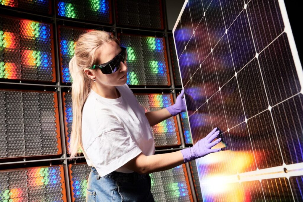
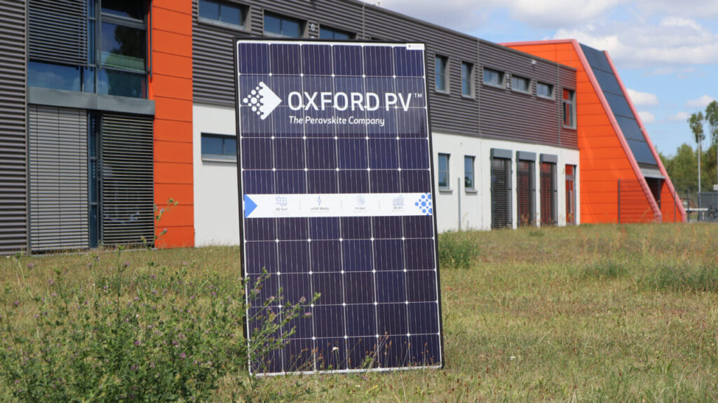
In September 2024, British perovskite tandem solar company Oxford PV shipped the world’s first commercial tandem solar modules. CEO David Ward heralded the moment as “a breakthrough for the energy industry” that would open the door to readily available, higher-efficiency solar products.
As a dedicated perovskite firm, Oxford PV has bet proportionally more on perovskite as the “next big thing” in solar technology than almost anyone else, but they have by no means been alone in their efforts.
Attending the Intersolar Europe conference earlier this year, PV Tech Power saw perovskite offerings from almost all the major solar manufacturers and a wide range of smaller ones.
Shortly thereafter, the 15th edition of the International Technology Roadmap for Photovoltaics (ITRPV) forecast that silicon-based tandem solar modules with 27% conversion efficiency would enter the mass market in 2027.
Effectively every major solar manufacturer has funded or been involved in research projects looking at perovskite-silicon tandem cell structures, from thousands-strong Chinese research and development (R&D) teams to European Union-funded projects involving technical institutions and universities.
Perovskite has become a white whale for the solar industry. It promises far higher light conversion efficiencies and less energy-intensive production than current silicon products, which could transform global solar module production and performance. But attaining those things means taming perovskite’s volatile nature, a feat that has so far eluded the industry.
This article draws on comments from leading figures in perovskite research and its sceptics to examine the technology, its possible commercialisation and the challenges the material poses.
The technology
Calcium titanate – more widely known as Perovskite – was first discovered in 1839 in the Ural Mountains. 170 years later, in 2009, its first application in a solar cell was reported by Tsumoto Miyasaka in Japan. This was a small, ink-based perovskite cell with around 3% efficiency.
Since then, a number of other materials similar to calcium titanate have been deployed in increasingly efficient solar cell configurations, which now reach up to the low 30 percents. This is a rapid technological evolution.
The most common iteration today is the perovskite-silicon tandem cell, which layers crystalline silicon technology and perovskites in a single cell. Generally, the perovskite layer sits on top of the base layer and increases the range of light that the cell can absorb and turn into power.
“There’s thin-film technology such as cadmium telluride and there’s waferbased [silicon] technology,” says Fabian Fertig, director of global R&D for wafers and cells at the German base of Korean-owned solar manufacturer Hanwha Qcells. “Both of these have a single junction and the theoretical efficiency potential is somewhere south of 30%.”
A junction is where electrical currents flow in a solar cell, between the positive and negatively charged layers.
Fertig continues: “Then you can look at different tandem configurations, and in principle, you can combine anything which has two different band gaps.”
A band gap determines the range of the light spectrum which a material can convert into electrical current. “It depends on how well this matches the solar spectrum to determine the efficiency potential,” he says.
“The advantage of perovskite is that the band gap is relatively widely tunable. By using different compositions in how you put your crystal together, you can absorb different light energies over a pretty wide range. The combined band gap of silicon – which is fixed – together with the tunable top cell band gap is pretty close to the theoretical optimum for any solar cell with two junctions.”
Variations on a theme
Fertig is involved in the PEPPERONI project, an EU-funded scheme developing a pilot line for silicon-perovskite tandem cell and module production. The project uses Q.ANTUM technology developed by Qcells for its silicon bottom cell, which has proven long-term durability over many years.
“Silicon has shown it’s mature and is dominating the world market, so you can use this manufacturing base, then build a solar cell on top and then chuck this into a system with high efficiency. We see that as the most promising option at the moment,” Fertig says.
The PEPPERONI project is working on a two-terminal tandem cell, rather than a four-terminal product. Two-terminal tandems lay perovskite directly onto a silicon base layer within the same cell; four-terminal products fabricate a thin-film cell for the perovskite and pair that with a separate silicon-based cell.
Fertig explains that this decision is aimed at functionality and scaling into significant manufacturing: “We manufacture Q.ANTUM technology, which is dominating the world market [along with other silicon products]. So our approach is to use this as the bottom cell with the perovskite directly on top – that way, you can use similar module design, similar system components, etc., to move forward.”
Oxford PV, which shipped the first commercial perovskite tandem modules earlier last year, has also adopted two-terminal tandem technology because of its scalability.
According to deputy CTO Ed Crossland, having originally worked on a perovskite-only product, the company “decided early on to piggyback on silicon technology” and create tandem cells.
Crossland says of the advantage of the two-terminal approach: “Apart from the production simplicity, it looks exactly like the cell did before, so you can then more easily integrate that cell technology into existing module technologies for silicon.”
Oxford PV’s current technology is based on a heterojunction technology (HJT) bottom cell. “The heterojunction cell…has the simplest integration with a thin-film tandem,” he says. “When you take a two-terminal approach, the two cells need to be electronically linked together, and the heterojunction cell is very well suited to that. It already has the right conducting top electrodes to integrate a thin film tandem on top of.”
Crossland explains there was also an element of timing in the decision, as HJT seemed to be emerging as the dominant high-efficiency technology when Oxford PV was developing its tandem modules.
“In the meantime…TOPCon technology has come in and you can get very close to – maybe even as good as – those heterojunction potentials. But it turns out that there are ways now that have been developed and are not actually that tricky which make TOPCon a compatible bottom cell with perovskite as the thin film absorber.”
Alternative routes
US-based perovskite firm Caelux produces a perovskite-layered glass product, which it says can be applied to silicon modules. It’s a four-terminal product which the company claims can be combined with any crystalline silicon base cell.
“Caelux believes that four-terminal devices are more cost-effective and easier to scale than two-terminal devices and avoid a key pitfall of two-terminal architectures – current matching,” says Caelux CEO Scott Graybeal.
“We do not have to engineer the substrate – it already exists in the form of readily available industrial float glass and we can work with any crystalline silicon cell type, which means we have a very large market.”
Graybeal claims that Caelux’s technology is “the lowest cost path to produce high-efficiency, durable perovskite cells”.
Opinion differs on this technological point. Crossland addresses the “pitfall” of current matching in his explanation of Oxford PV’s decision to choose two-terminal products:
“When you stack two cells that are directly integrated, you need to have the same current flowing through the two things because they’re in series. In doing that you limit the absolute theoretical limit [of efficiency] you can get to. But that’s a relatively minor limitation compared with the advantages you get with a two-terminal integration.”
Technology such as Caelux’s, with its one-size-fits-all style adaptation to existing module technologies, could ease the adoption of perovskite technology into silicon solar production. However, the major players in the space have mostly opted for dedicated perovskite-silicon tandem cells rather than active glass because of their adaptability to large-scale production.
Stability – ‘The nut to crack’
Crossland says that the first perovskite cells in university labs, usually around the size of a fingernail, had a lifetime of about an hour before there would be noticeable degradation in their performance. This is the factor that, more than any other, has held back perovskite-based solar products from entering the commercial mainstream. The material degrades when exposed to oxygen and moisture at a rate that has made it uncompetitive with silicon products, which can operate with very gradual degradation for 25-30 years.
Crossland says this means perovskite encapsulation requirements are far higher than other thin-film and silicon technologies, and tandem modules will need to be encapsulated in double glass, rather than using a back sheet on the rear of the product.
These represent two separate concerns in the product development process, which Crossland dubs “Atom to module”.
“We’ve got R&D teams which work on the fundamental stability of the perovskite absorber, understanding which chemical degradation routes exist and how you can improve them,” he says, “All the way up to the module manufacturing process, where you need to be careful what ambient moisture and exposure are given to the perovskite material if you want to end up with a cell and a module which is stable once it is encapsulated.”
The encapsulants themselves have been the subject of lab research, too. “In the early days, you couldn’t reach 100 degrees in your post-processing before the perovskite absorber had problems,” he says.
“That really limits what encapsulation method you can apply to your technology. So we’ve gone through the dual process of finding encapsulation materials that work in the 150-degree range and making the absorber and active materials inside the device intrinsically stable to those process temperatures so that they meet in the middle. You end up with a module technology that can be encapsulated to a degree that gives you a field lifetime as good as required.”
Innovations aside, the material’s stability still looms as a large caveat with every new perovskite or tandem cell efficiency record. Emily Warren, a scientist at the US National Renewable Energy Laboratory (NREL), says that stability is now more important than efficiency.
“We would rather have a record stability than record efficiency,” she says. “All the researchers need to ask if they want this to be a real technology. That means it needs to be sustainable and able to be manufactured reproducibly – and does that change your research versus trying to get a new efficiency and get [on the] cover of a journal?”
The route to commercialisation
A March 2024 paper from NREL lays out a list of “development needs” for perovskite products to come to mass market. Based on the ITRPV roadmap, it posits that cell and module R&D, reliability and scaling efforts, manufacturing developments and deployment evaluations need to be undertaken in tandem to get the technology out of the lab and into the real world.
This relies on collaboration and consortia like the PEPPERONI project and harnessing the infrastructure and technology of mature PV technologies. This is the principle behind choosing the two-terminal silicon-tandem technologies discussed above.
Crossland claims that everything Oxford PV does is ultimately geared toward large-scale production. “Like with the two-terminal selection…we would apply thin-film scaling techniques and tools that already existed, so many of the problems you’d have to solve with something new were already solved. Wherever possible, we picked scalable processes that were already there.”
“We want to move past silicon”
During the production process of this magazine, researchers from the University of Surrey in the UK published findings that they claimed increased the stability of perovskite-perovskite tandem solar cells.
Pure perovskite products are the next frontier after silicon-perovskite tandems. They offer even higher efficiencies than tandem products, as they are unbound by silicon’s fundamental physical limits, but also untethered from its physical reliability. Where silicon tandem products have recently begun to meet the market, perovskite-perovskite solar is at the cutting edge of research.
“Ultimately, we want to move past silicon”, says Hashini Perera of the Advanced Technology Institute at the University of Surrey, lead author of the recent research. “The whole reason we are talking about perovskite is that the extraction of silicon is an energy-intensive process and the cost factor is there.
“Silicon has already proven it can be stable for 25 years… so if we want to replace it, we need a perovskite which can do the same job.” As well as stability, this perovskite also needs work on a narrow band gap to absorb the same range of light as silicon.
Perera’s research used a perovskite with both lead and tin added, which she says is needed to achieve a narrow band gap. But tin oxidises quickly, which can reduce cell efficiency and stability. The findings showed that a particular additive (thiocyanate), which had been added to perovskiteperovskite cells for years to stabilise their performance in lab conditions could actually accelerate the degradation of cells in real-world surroundings.
The findings encapsulate the central question of all perovskites: efficiencies vs durability.
“If it is in a very inert environment, the additive can improve performance, but if there is even the slightest bit of moisture ingress it can kill the device,” Perera says.
“The additive was added to improve the performance, but when you test the stability it is degrading much faster than without the additive.”
Perera’s paper claims to have extended the lifespan of perovskite-perovskite cells by up to 60%; potentially a significant step towards the next frontier of cell technology.
For example, he says that thin-film and silicon manufacturing have increased productivity massively in recent years, “essentially by making the tools bigger. So you can coat [deposition materials] on a bigger area, and you get more wafers per hour…your productivity goes up, your unit cost goes down. We’ve already started with platforms which are essentially smaller versions of those tools.”
Oxford PV has said it plans to establish gigawatt-scale manufacturing at its facility in Brandenburg, Germany, which would be the first mass production of perovskite tandems anywhere.
Broad collaboration will also be important. Warren, one of the authors of the NREL paper above, tells PV Tech Power that reliable product testing and available data around perovskite tandems will be an important part of the commercialisation process.
“At the end of the day, anyone who is going to install a solar array is interested in the total amount of kilowatt hours of electricity made. That is not [cell] efficiency,” she says. Important data like the LCOE of a PV project are tied to predicting how a product or technology will perform in a given environment over its lifespan.
“There’s a whole industry that exists for energy yield prediction,” she says, “The problem is that none of the tools available right now incorporate the differences of having a tandem, where you have two different band gaps and two different materials within a module.”
Such a tool would allow tandem solar products to answer the inevitable questions posed by technology backers and financiers—namely: “ How much energy will this produce?”
“All thin-film materials [including perovskites] show some level of metastability. That makes it extra hard,” Warren says. “It’s not the same as silicon where you can model it once, and it will be the same today, tomorrow and the next day. That’s never true in a thin film.”
Warren says she would like to see a third-party validation and testing system for perovskite tandem products to allow the technology to progress. “The community needs data sets of how these things are performing to make sure we can predict how the next one will perform,” she says.
Ed Crossland says similarly: “You do better when you collaborate. We’re engaging with partners by licensing our IP…partnerships with development, partnerships with production, and I think that’s the right way to approach rapid deployment of this technology.”
Early markets
Fertig insists that there is no reason the potential of laboratory perovskite products can’t be replicated on more commercially viable products. He says the efficiency is clearly there, but questions remain over durability and cost—but those questions are not unanswerable.
“We will have to see if all market segments require the same long-term stability as silicon, or whether there might be some which say they can accept a higher performance without the same reliability requirements,” he says.
Niche applications like aerospace or flexible products, where modules need to be as efficient as possible relative to both size and weight, would be logical steps for perovskite technology. But those products represent a vanishingly small blip on a map of the global solar market. Stepping into rooftop and, ultimately, utility-scale deployments is a different challenge altogether.
Is perovskite the next c-si?
Silicon technology has become incredibly cheap and abundant and has emerged as the dominant energy transition technology. It’s unclear whether perovskite has the potential to take over that mantle.
For Fertig, the outlook is simple: “Either it will be competitive, or it won’t.
“In the history of PV there has always been a product that’s been dominating the market. Then, at some point, a new technology comes around, and either it’s superior to the old technology or it’s not. The latest example is TOPCon.”
Perovskite’s higher efficiencies can push past the limits of silicon, which Fertig says could dethrone the old technology.
Crossland is more strident; “Of course it will be the dominant technology. Why wouldn’t it be? Why wouldn’t you pick a higher efficiency technology that fits inside the same product form that you have before?”
Oxford PV is aiming for a 1% annual degradation rate in its tandem modules, which it has yet to achieve. But Crossland says there is no fundamental reason why perovskite tandem cannot become the next dominant technology: “We have proof of principle in small areas that we can reach those kinds of annual degradation rates – not yet in the full product, but we will do it.”
For Warren, perovskite tandem products offer a way to diversify the global solar supply chain and ease the pressure that has arisen through its overwhelming reliance on one material (polysilicon) produced in a few locations.
“The final product is a really big, flat thing which contains glass,” she says. “Making that locally seems like a good idea.
“Perovskite and other thin-film technologies have a different supply chain and manufacturing footprint. We need a lot of material to continue the growth trajectory of solar, so I would say that I’m in favour of all the technologies. [Perovskite] is not necessarily going to displace silicon any time soon, but having a more diverse supply chain is going to greatly enhance the ability of the PV industry to grow.”
Radovan Kopecek, the founder of ISC Konstanz and a long-standing figure in the crystalline silicon manufacturing industry, is sceptical, denouncing what he describes as “perovskite populists” who have grabbed headlines with efficiency records that have yet to bear any industrial fruit.
“It’s easier to sell efficiencies than complex bankability,” he says. “People say when there’s a 27% efficiency module everyone will buy it – it’s nonsense. You have to look at the whole picture.”
Kopecek’s argument is that crystalline silicon solar technology, in conjunction with energy storage, will be the lowest-cost electricity source available and will drive the energy transition. “We don’t need any hocus pocus that will potentially lower costs because we are already there.”
He cites data, which will be published in an upcoming article he has co-written, showing that existing solar technologies will provide the cheapest LCOE everywhere in the world besides Scandinavia by 2030. Indeed, the average selling price of silicon-based solar modules has declined massively over the last two years, and the glut of manufacturing capacity may prevent it from rising much in the near future. The prices of BESS are also declining.
For Kopecek, the pendulum in Europe has swung away from industrial knowledge and experience towards scientific operations in laboratories. This is an issue, he says, because solar PV has become a mainstream, commoditised technology where the research now goes into system and module-level tweaking, rather than the fundamental building blocks of the technology.
Fundamentally, he believes that by the time perovskite products are ready to meet mainstream market demand, that demand will have been met by low-cost and abundant silicon and energy storage products.
“I’m quite sure that they will make their way into the market, but there is no way they will drive our energy transition,” he tells us.
However, it is not just technological scepticism that makes Kopecek so “emotional” (as he puts it) about the trend towards perovskite research.
“The energy transition is really about terawatt-scale production of crystalline silicon solar technology and we cannot just depend on one or two countries like China and India,” he says. “We [in Europe] must do it ourselves. For many years we have delivered the wrong message; ‘we have lost the crystalline silicon battle, but we will go to perovskite which is the new big thing.’ It is not.”
The Libertas project in Germany, in which Kopecek’s ISC Konstanz was involved, has been investigating the feasibility of restoring a silicon solar manufacturing industry to Germany. He tells PV Tech Power that the project was hamstrung by discussions and deliberations over technology and the module efficiency needed for an economically viable product, to the point that it missed the window for funding in the German budget.
Kopecek claims that “some lobbyists for new tech” pushed for the technological change. “This is what is making me extremely angry,” he says, pointing to a similar influence of thin-film “lobbyists” in the US that have pushed for funding towards perovskite research.
In contrast to Emily Warren from NREL, who sees perovskite as a means of diversifying the solar supply chain away from China, Kopecek sees it as a roadblock to bringing silicon capacity onshore in the West, and Europe in particular.
Fabian Fertig says there are “Always people who say that new technology is never going to work. I’m confident, looking at the technological details, that there’s a good chance, and Europe does have an edge in [perovskite] technology.”
For Fertig (who works for Qcells, a silicon solar manufacturer), the macroeconomic situation has done more to prevent Europe from creating a meaningful manufacturing base than perovskite R&D. He says that while he “is not an economist”, the current selling price for silicon modules is too low to support European production.
“If we look at technologies where Europe is at the forefront, where we are ahead of other markets, I would say money spent on perovskite-on-silicon is money well spent.”


