Swiss-based PV manufacturing equipment specialist INDEOtec SA has been carving out a key role in the emerging PECVD-PVD deposition market for next-generation heterojunction (HJ) solar cells. INDEOtec had been a key sponsor of the inaugural PV CellTech conference in 2016 and once again has chosen the event to be a major showcase for its technology and expertise.
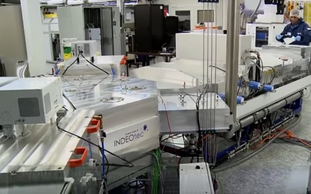
The company has supplied multiple ‘OCTOPUS’ PECVD-PVD cluster systems to various renowned solar R&D facilities around the world that are supporting advanced research into HJ technology. The ‘OCTOPUS’s PECVD’ is used to deposit intrinsic and doped amorphous silicon (a-Si:H) materials as well as for passivation processes using Si alloys such as SiNx, SiOx, and OCTOPUS’s PVD is used to deposit TCOs and metallic thin layers such as ITO, AZO, ZnO, Ag and Al.
Try Premium for just $1
- Full premium access for the first month at only $1
- Converts to an annual rate after 30 days unless cancelled
- Cancel anytime during the trial period
Premium Benefits
- Expert industry analysis and interviews
- Digital access to PV Tech Power journal
- Exclusive event discounts
Or get the full Premium subscription right away
Or continue reading this article for free
In January 2017, INDEOtec was awarded an important grant from the SWISS Commission for Technology and Innovation (CTI) to further develop its OCTOPUS II platform in partnership with Swiss research partner, CSEM.
A key part of the funding was to support further validation of its OCTOPUS II cluster system for double-sided HJ deposition requirements, enabled by its unique ‘PECVD-Mirror Reactor’ design that offers lower processing costs and higher conversion efficiencies for heterojunction solar cells, The Mirror Reactor concept enables the top and bottom side thin film substrate deposition without the need of substrate flipping and vacuum breakage that can cause cell performance loss and manufacturing complexity. Another key element of the funding is the validation of ACCT or Anti-Cross-Contamination Treatment, a special knowledge developed by Indeotec to radically solve the issue of intrinsic a-Si contamination by n- & p- dopants from either contaminated reactor walls or contaminated carrier plates. ACCTenables stack layers deposition of intrinsic and doped a-Si with the same carrier plate and therefore, in the same PECVD reactor and simplifying even further handling steps inside the PECVD machine.
Dr. Omid Shojaei, CEO of INDEOtec SA gave PV Tech a sneak insight into its next-generation OCTOPUS III platform that is currently in development that can take R&D and pilot production HJ cells into volume production. Dr. Shojaei has also been a member of the PV CellTech advisory board and presenting at this years PV CellTech event.
“We regard the OCTOPUS II cluster system the bridge between R&D and pilot line production, which is capable of 6MW of heterojunction (HJ) solar cells,” noted Dr. Shojei. “However, we are readying the jump to a mass production platform, named OCTOPUS III – PECVD with an initial throughput of 2,400WPH capability. This comes from larger reactor sizes but retaining all the benefits of Mirror Reactor design and ACCT including the elimination of cross contamination of conventional PECVD tools on the market.”
“With OCTOPUS II we could handle four wafers on the plate but with OCTOPUS III will initially be able to process 48 wafers at the same time.”
The need to develop a mass production platform is evident by the recent momentum in next-generation HJ cell technology and commercialisation.
“We clearly see but without disclosing the names that there are more and more opportunities that are coming from China as well as other regions. But what we also feel is that cell producers want to buy proven technology that has shown at least 23% average cell efficiency in a pilot scale. This puts the risks back on the equipment supplier and we need to bring breakthrough technologies at an acceptable level of price to satisfy their requirements.”
There are many improvements in term of cell structures and efficiency potential, however, challenges with HJ technology also exist in areas outside the control of the equipment suppliers according to Dr. Shojaei.
“A key challenge we see is in the supply and intrinsic quality of the wafer, unlike that required for say PERC based solar cells. With the deposition of multiple layers at only 8 to 10 nanometres thick with heterojunction cells the quality of the wafer is extremely important. Heterojunction cells require the best wafer uniformity on the features.”
“The second challenge is clearly on the PECVD side with complexity of automation and process cross contamination, due to wafer handling within the system. By avoiding touching the wafer this would help in this issue.”
However, Dr. Shojaei also noted that key challenges also exist at the module assembly end, in particular the tabbing and stringing, due to process temperatures often in the 400C degree level when HJ cells can only cope with temperatures around 200C levels. There are various alternative solutions that are proposed today, but we feel there should more effort of validation and price reduction.
To view the final PV CellTech agenda updates, please follow this link. To register for the event, click here.


