Move over pesky perovskites and old faithful intrinsic amorphous silicon as the preferred solutions for tandem-junction solar cell post crystalline-silicon PERC (passivated emitter rear cell) technology: A perennial conversion efficiency record holder and space-proven solution is back to gate-crash the party.
Gallium arsenide (GaAs) or III-V materials in a single-junction device have a proven history of efficiency records. For example, Alta Devices achieved conversion efficiencies of 28.8% on such a device more than six years ago and hit efficiencies of 31.6% on a dual-junction thin-film solar cell format in 2016.
Try Premium for just $1
- Full premium access for the first month at only $1
- Converts to an annual rate after 30 days unless cancelled
- Cancel anytime during the trial period
Premium Benefits
- Expert industry analysis and interviews
- Digital access to PV Tech Power journal
- Exclusive event discounts
Or get the full Premium subscription right away
Or continue reading this article for free
The biggest challenge with growing III-V materials has been the production costs. Even when using sacrificial wafer substrates, the production costs for PV cells using such materials come in well above commercial cost levels for mainstream terrestrial solar cells.
Several years ago, a promising technology to manufacture gallium arsenide nanowire arrays by Swedish start-up Sol Voltaics caught my attention. The company didn’t tout big-league conversion efficiencies (15.3% actual) or claim low-cost roll-to-roll capabilities (in fact, they don’t even use a roll-to-roll process). Instead, they touted their in-house Aerotaxy nanowire production method that, if scaled, could dramatically cut production costs and boost efficiencies.
Ever since my first introduction to the technology, PV Tech has covered Sol Voltaics when it has had something to say. But as with many start-ups, there can be long gaps between announcements, and companies may or may not publicise breakthroughs or discuss cautious progress toward their commercialisation goals.
In contrast to those overhyped pesky perovskites, Sol Voltaics’ Aerotaxy nanowire thin-film reactor process and commercial tool development has continued at a relatively brisk pace. The company has maintained its cautious confidence in achieving a production-ready tandem cell that enhances overall module efficiency by more than 50%, which would enable module conversion efficiencies above 27%.
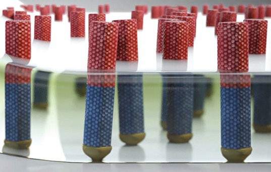
The nanowires formed in Aerotaxy process are grown in a way that the top and bottom of the nanowire have opposite doping profiles and form a solar cell with p-n junctions found along the length of the individual nanowires. However, the orientation of nanowires can be problematic. But in recent years, Sol Voltaics has developed films (SolFilm) that act as a transfer mechanism and correctly orient the nanowires to be used as a tandem layer and allow them to be transferred to a crystalline-silicon cell.
This is a critical development in Sol Voltaics’ path to commercialisation or at the very least enables the correct alignment of GaAs nanowire film so that solar cell and module producers can evaluate costs and conversion efficiency gains. It’s similar in principle to the likes of Oxford Photovoltaics establishing an evaluation centre to run its perovskite samples on customer cells.
So how close do I think Sol Voltaics is to its commercialisation goals?
My best guess would have been three to five years from now. But I’d add a few more years unless a series of publicly issued updates on progress toward commercialisation suggest otherwise. For many other promising start-up technologies, a lack of updates often has meant goals have been pushed out a few more years. When this happens, the companies are usually in no hurry to talk to journalists and discuss their lack of progress.
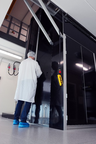
So when I was invited to come and see Sol Voltaics’ progress toward commercialisation first hand, I was pleasantly surprised. Not only did the company offer a tour of a newly completed facility built to initiate commercial activities as well as a peek inside its new qualification lab, the trip was only a quick hop, skip and jump from London to Lund University’s technology campus in Sweden.
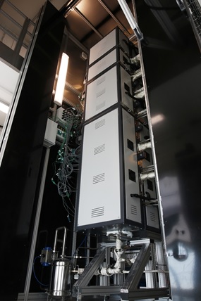
During the tour, I was impressed by the scale of the current Aerotaxy chamber (see below). This isn’t a small sample spin-on glass perovskite lab; although the images show only the outside of the chamber, inside it features completely industrial specified components and a pre-volume production layout. The true volume production tool is deep in the design phase, where it is undergoing rigorous design iterations
Another factor in Sol Voltaics’ favour is that the GaAs nanowires only need to coat around 20% of the c-Si cell surface to generate claimed efficiency gains, rather than the full 100% coating necessary in other technologies. This is not the only significant cost-saving part of the process: the Aerotaxy system can fully recycle the materials used.
The production testing and qualification lab has been installed with a suite of tools required to support GaAs nanowire processing when the production tools are built and put into operation. Space exists in the facility for a given quantity of SolFilm substrates, and layout plans were being tweaked during my visit to the Lund facility.
So how close does Sol Voltaics think it is to its commercialisation goals?
Volume production of the nanowires is only a couple of years away, according to CEO Erik Smith. The company has already achieved repeatable nanowire alignment and orientation through the development of the SolFilm substrate process. The company remains on track to start providing samples of its SolFilm to potential partners by the end of 2018/early 2019, he added.
Understandably, Smith and the rest of the Sol Voltaics team are hesitant to give volume production process costs away. But the scale and the pace of the operations moving to commercialisation are impressive to see.
Investors would seem to agree. The company recently secured US$21.3 million in a new funding effort from a number of previous round investors, including Kagra Gruppen AS Nordic VC firm Industrifonden, FAM AB, Nano Future Invest, Blue Marlin AB, Teknoinvest AS and new investor Watrium AS.
As with any technology start-up, caution should be applied when talking up Sol Voltaics’ ability to get through the “Valley of Death” phase (taking technology from the lab to the fab) or establishing timelines post-VoD that predict the first volume orders. However, it would also be prudent to include GaAs nanowire film technology as a next-generation tandem-junction product offering in the same way that heterojunction and perovskite materials are touted today.


